Compliance Measurement
Transmitter testing can be easily performed by using the various test patterns listed in Figure 4 (link to [Things You Know and Don't Know About USB2.0, USB3.0 Structure and Test]). Each pattern is selected for characteristics related to the test that evaluates the pattern. CP0 (D0.0 scrambling sequence) is used to measure deterministic (Dj) jitter, such as data-dependent jitter (DDJ); CP1 (D10.2 full-rate clock pattern without scrambling) does not produce DDJ and is therefore more suitable for evaluating random jitter (Rj).
Jitter and eye height are measured using 1 million continuous unit intervals after applying the equalizer function and the corresponding clock recovery settings (second-order PLL, 10 MHz closed-loop bandwidth, and 0.707 damping factor). The jitter results are calculated, which exceed the total amount of measured data samples and quickly extract the specific jitter performance at the 1 x 10-12 BER level. For example, in jitter extrapolation, the target Rj can be calculated by multiplying the measured Rj (rms) by 14.069. Figure 6. Transmitter test points.

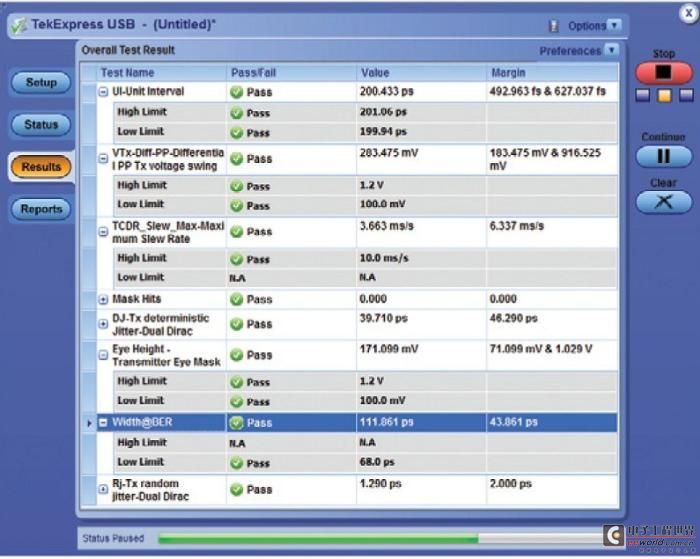 Figure 7. DPO/DSA70000 Series Option USB-TX for USB 3.0 normative and informative measurements.
Figure 8. USB 3.0 debugging using DPOJET, including custom control setup.
Figure 6 shows the standardized transmitter compliance test setup, including the reference test channel and cable. Test point 2 (TP2) is closest to the device under test (DUT), while test point 1 (TP1) is the measurement point at the far end. Note that all transmitter standardized measurements are performed on the signal at TP1.
After acquiring the signal at TP1, the data is processed using a software tool called SigTest, which is similar to the official PCI Express compliance test. For applications that require pre-compliance testing, characterization, or debugging, additional tools can be used to further understand the design behavior under varying conditions or parameters. A Tektronix MSO/DPO/DSA70000 Series oscilloscope with Option USB-TX can perform all USB 3.0 normative and informative physical layer transmitter tests, as shown in Figure 7. Single-button automated software tools, such as USB-TX, save time by ensuring that the test equipment is configured correctly. Lab technicians can accurately run tests, rather than senior engineers with in-depth knowledge of the USB specification. At the end of the test, detailed pass/fail reports will list where design problems may have occurred. If different test locations (such as corporate labs, test houses, etc.) get conflicting results, tests can be run using data saved from previously run tests.
TekExpress test automation software with option USB-TX leverages the characterization and debug environment based on the common analysis capabilities of DPOJET. Flexible jitter and eye diagram analysis packages provide more user-defined control over analysis parameters, helping to speed up the debug process and greatly simplify design characterization. For example, multiple eye diagrams can be displayed at once, allowing users to analyze the effects of different clock recovery techniques or software channel models. In addition, different filters can be applied to analyze the effectiveness of SSC in addressing system interoperability. Figure
9. ISI board with 12-inch and 24-inch traces. [page]
Figure 10. Magnitude and phase response of 12-inch and 24-inch PCB traces.
Reference Test Channels
The "far end" signal at TP1 can be captured in two ways. The first method uses the USB-IF hardware-based cable and fixture to acquire data at TP1. The second approach uses a model extracted from a TDR, VNA, or simulator to simulate the hardware channel effects in software. The commonly accepted channel model is an S-parameter file that includes both magnitude and phase response effects. The signal is acquired at TP2, or closest to the transmitter, and the acquired data is convolved with the S-parameter file, which has been converted into a finite impulse response (FIR) filter (for more information on filter applications on Tektronix oscilloscopes, refer to the white paper “Principles, Design, and Application of Arbitrary FIR Filters” on www.tektronix.com).
This approach allows engineers to measure the device under test with varying and repetitive specific channel requirements. For example, let’s compare the measurement results of a 5 Gb/s signal in different PCB trace lengths. Figure 9 shows the ISI test board connected to 12-inch and 24-inch traces, and Figure 10 provides the corresponding Sdd21 channel response.
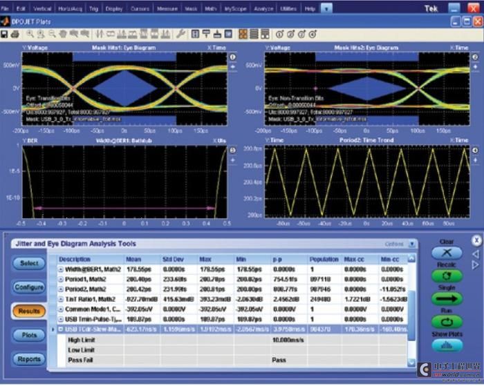
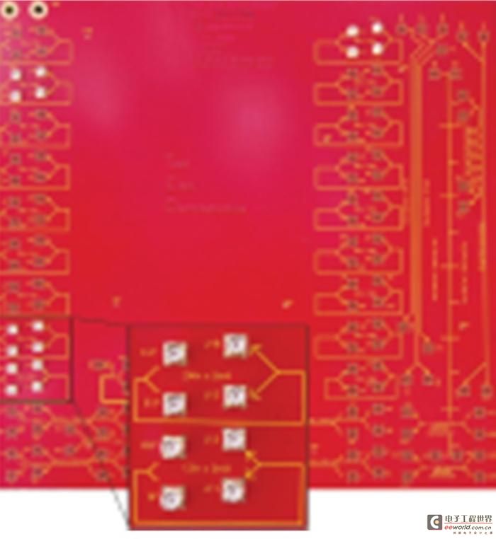
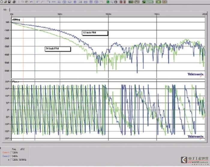
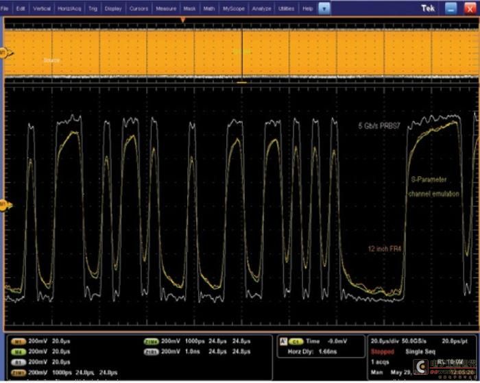
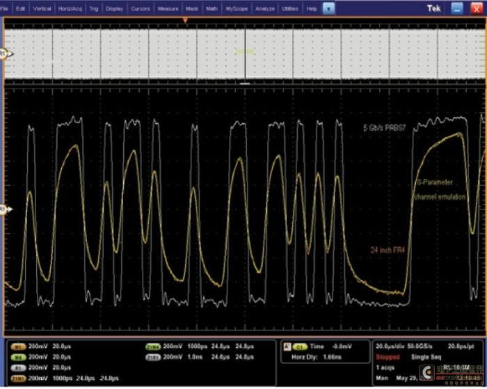
Figure 12. Hardware channel simulation and software simulation of a 24-inch track.
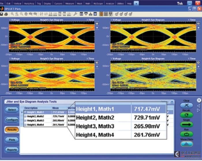 Figure 13. 5 Gb/s eye diagrams after 12-inch and 24-inch traces, hardware-emulated channels (left) and software-emulated channels (right).
Test signals were acquired both when the hardware channels were included and when they were not. Figures 11 and 12 show the original signal (white), the far-end hardware response (orange), and the original signal after convolution with the S-parameter data for each trace length. Figure 13 includes eye diagrams from both hardware-based and software-based test data. [page]
Equalization
Due to significant channel attenuation, SuperSpeed USB requires some form of compensation to open the eye at the receiver. To achieve this, equalization (in the form of de-emphasis) is used on the transmitter. The nominal de-emphasis ratio is specified to be 3.5 dB, which is 1.5x when using a linear scale. For example, when the transition bit level is 150 mV pk-pk, the non-transition bit level will be 100 mV pk-pk.
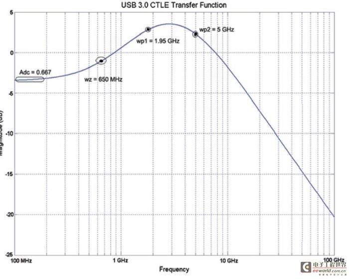
The conforming equalization model is a continuous time linear equalizer (CTLE). CTLE implementations include on-chip filters, active receiver equalization filters, or passive high-frequency filters such as those found in cable equalizers. This model is particularly well suited for compliance testing because it can simply describe the transfer function. The CTLE is implemented in the frequency domain using a set of poles and zeros to produce a peak at the desired frequency. As mentioned earlier, TekExpress software with option USB-TX includes the reference compliance channel as well as the required CTLE filter, all combined into one file. Figure 14. USB 3.0 CTLE transfer function and magnitude response.

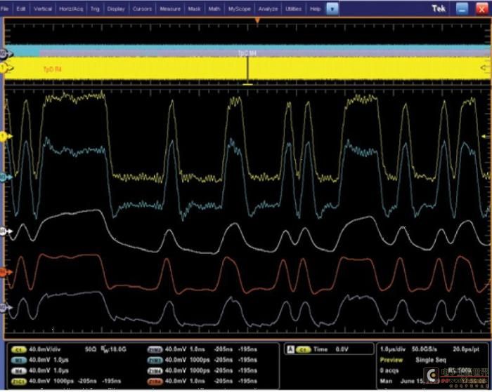
In addition to using the compliance filters provided in the TekExpress automation software, designers can use the Tektronix Serial Data Link Analysis (SDLA) software to verify different CTLE parameters and their impact on link performance. The advantages of CTLE implementations are that they are simpler to design and consume less power than other solutions. However, in some cases, they may not be sufficient due to limitations in adaptability, accuracy, and noise amplification. Other techniques include feed-forward (FFE) equalization and decision feedback (DFE) equalization, which use data samples weighted with a scale factor to compensate for channel losses. Both CTLE and FFE are linear equalizers, so both experience signal-to-noise ratio degradation, which manifests as increased high-frequency noise. However, DFE uses nonlinear components in the feedback loop, thereby minimizing noise amplification and compensating for ISI. Figure 16 shows a 5 Gb/s signal after significant channel attenuation, and the signal after equalization using de-emphasis, CTLE, and DFE techniques.

Characterization and Debug
Throughout the design verification and compliance testing process, debug tools are always needed to resolve signal integrity or jitter issues. As circuit margin degradation increases complexity and link issues, chip designers and system integrators need tools with intelligent statistical analysis capabilities and visualization tools such as histograms, jitter spectra, and BER "bathtub" curves. DPOJET analysis plots, such as spectrum plots and trend plots, provide in-depth information beyond simply displaying measurement data and results. Trend analysis shows how timing parameters change over time, such as frequency drift, PLL startup transients, or circuit response to power supply changes. Jitter spectrum analysis can show the exact frequency and amplitude of jitter and modulation sources (neighboring oscillators and clocks), power supply noise, or signal crosstalk.
After a test failure, it is very important to be able to switch from "compliance mode" to "user-defined" jitter and eye diagram analysis tools using the automated test software. With DPOJET software, users can control parameters such as clock recovery, filtering, reference levels, Rj/Dj separation techniques, or measurement limits and gating. In addition to the specified standardized USB 3.0 measurements and informative USB 3.0 measurements, it includes many timing, amplitude, and eye diagram measurements.
Figure 17 shows an example of a procedure for debugging and analyzing jitter. First, we acquire data using a relatively large data sample size to perform jitter analysis, including the effects of SSC. A 33 kHz SSC period requires a 30 us time window. Once the data is acquired, eye diagram analysis can quickly provide a visual indication of voltage and timing performance. This eye diagram shows that period jitter and data-related jitter are excessive. Finally, we perform jitter decomposition to isolate signal integrity issues. The jitter spectrum plot highlights the jitter components and their corresponding relative amplitudes and frequencies. Figure 18. USB 2.0 and 3.0 receiver test example.

Reference address:Teach you how to test USB3.0 transmitter step by step
Transmitter testing can be easily performed by using the various test patterns listed in Figure 4 (link to [Things You Know and Don't Know About USB2.0, USB3.0 Structure and Test]). Each pattern is selected for characteristics related to the test that evaluates the pattern. CP0 (D0.0 scrambling sequence) is used to measure deterministic (Dj) jitter, such as data-dependent jitter (DDJ); CP1 (D10.2 full-rate clock pattern without scrambling) does not produce DDJ and is therefore more suitable for evaluating random jitter (Rj).
Jitter and eye height are measured using 1 million continuous unit intervals after applying the equalizer function and the corresponding clock recovery settings (second-order PLL, 10 MHz closed-loop bandwidth, and 0.707 damping factor). The jitter results are calculated, which exceed the total amount of measured data samples and quickly extract the specific jitter performance at the 1 x 10-12 BER level. For example, in jitter extrapolation, the target Rj can be calculated by multiplying the measured Rj (rms) by 14.069. Figure 6. Transmitter test points.


Figure 11. Hardware channel simulation and software simulation of a 12-inch track.

Figure 12. Hardware channel simulation and software simulation of a 24-inch track.

Test signals were acquired both when the hardware channels were included and when they were not. Figures 11 and 12 show the original signal (white), the far-end hardware response (orange), and the original signal after convolution with the S-parameter data for each trace length. Figure 13 includes eye diagrams from both hardware-based and software-based test data. [page]
Equalization
Due to significant channel attenuation, SuperSpeed USB requires some form of compensation to open the eye at the receiver. To achieve this, equalization (in the form of de-emphasis) is used on the transmitter. The nominal de-emphasis ratio is specified to be 3.5 dB, which is 1.5x when using a linear scale. For example, when the transition bit level is 150 mV pk-pk, the non-transition bit level will be 100 mV pk-pk.
The conforming equalization model is a continuous time linear equalizer (CTLE). CTLE implementations include on-chip filters, active receiver equalization filters, or passive high-frequency filters such as those found in cable equalizers. This model is particularly well suited for compliance testing because it can simply describe the transfer function. The CTLE is implemented in the frequency domain using a set of poles and zeros to produce a peak at the desired frequency. As mentioned earlier, TekExpress software with option USB-TX includes the reference compliance channel as well as the required CTLE filter, all combined into one file. Figure 14. USB 3.0 CTLE transfer function and magnitude response.


Figure 15. SDLA equalization configuration for CTLE, FFE, and DFE.

Figure 16. 5 Gb/s signal (yellow) after de-emphasis (blue), long channel (white), CTLE (red), and 3rd-order DFE (grey).
In addition to using the compliance filters provided in the TekExpress automation software, designers can use the Tektronix Serial Data Link Analysis (SDLA) software to verify different CTLE parameters and their impact on link performance. The advantages of CTLE implementations are that they are simpler to design and consume less power than other solutions. However, in some cases, they may not be sufficient due to limitations in adaptability, accuracy, and noise amplification. Other techniques include feed-forward (FFE) equalization and decision feedback (DFE) equalization, which use data samples weighted with a scale factor to compensate for channel losses. Both CTLE and FFE are linear equalizers, so both experience signal-to-noise ratio degradation, which manifests as increased high-frequency noise. However, DFE uses nonlinear components in the feedback loop, thereby minimizing noise amplification and compensating for ISI. Figure 16 shows a 5 Gb/s signal after significant channel attenuation, and the signal after equalization using de-emphasis, CTLE, and DFE techniques.

Figure 17. DPOJET software for advanced serial data characterization and debug.
Characterization and Debug
Throughout the design verification and compliance testing process, debug tools are always needed to resolve signal integrity or jitter issues. As circuit margin degradation increases complexity and link issues, chip designers and system integrators need tools with intelligent statistical analysis capabilities and visualization tools such as histograms, jitter spectra, and BER "bathtub" curves. DPOJET analysis plots, such as spectrum plots and trend plots, provide in-depth information beyond simply displaying measurement data and results. Trend analysis shows how timing parameters change over time, such as frequency drift, PLL startup transients, or circuit response to power supply changes. Jitter spectrum analysis can show the exact frequency and amplitude of jitter and modulation sources (neighboring oscillators and clocks), power supply noise, or signal crosstalk.
After a test failure, it is very important to be able to switch from "compliance mode" to "user-defined" jitter and eye diagram analysis tools using the automated test software. With DPOJET software, users can control parameters such as clock recovery, filtering, reference levels, Rj/Dj separation techniques, or measurement limits and gating. In addition to the specified standardized USB 3.0 measurements and informative USB 3.0 measurements, it includes many timing, amplitude, and eye diagram measurements.
Figure 17 shows an example of a procedure for debugging and analyzing jitter. First, we acquire data using a relatively large data sample size to perform jitter analysis, including the effects of SSC. A 33 kHz SSC period requires a 30 us time window. Once the data is acquired, eye diagram analysis can quickly provide a visual indication of voltage and timing performance. This eye diagram shows that period jitter and data-related jitter are excessive. Finally, we perform jitter decomposition to isolate signal integrity issues. The jitter spectrum plot highlights the jitter components and their corresponding relative amplitudes and frequencies. Figure 18. USB 2.0 and 3.0 receiver test example.

Previous article:Research on a printing detection method based on CAN bus
Next article:Factors that may cause damage to high-speed data transmission and analysis of the test process
- Popular Resources
- Popular amplifiers
Recommended Content
Latest Test Measurement Articles
- Keysight Technologies Helps Samsung Electronics Successfully Validate FiRa® 2.0 Safe Distance Measurement Test Case
- From probes to power supplies, Tektronix is leading the way in comprehensive innovation in power electronics testing
- Seizing the Opportunities in the Chinese Application Market: NI's Challenges and Answers
- Tektronix Launches Breakthrough Power Measurement Tools to Accelerate Innovation as Global Electrification Accelerates
- Not all oscilloscopes are created equal: Why ADCs and low noise floor matter
- Enable TekHSI high-speed interface function to accelerate the remote transmission of waveform data
- How to measure the quality of soft start thyristor
- How to use a multimeter to judge whether a soft starter is good or bad
- What are the advantages and disadvantages of non-contact temperature sensors?
MoreSelected Circuit Diagrams
MorePopular Articles
- LED chemical incompatibility test to see which chemicals LEDs can be used with
- Application of ARM9 hardware coprocessor on WinCE embedded motherboard
- What are the key points for selecting rotor flowmeter?
- LM317 high power charger circuit
- A brief analysis of Embest's application and development of embedded medical devices
- Single-phase RC protection circuit
- stm32 PVD programmable voltage monitor
- Introduction and measurement of edge trigger and level trigger of 51 single chip microcomputer
- Improved design of Linux system software shell protection technology
- What to do if the ABB robot protection device stops
MoreDaily News
- Industry first! Xiaopeng announces P7 car chip crowdfunding is completed: upgraded to Snapdragon 8295, fluency doubled
- P22-009_Butterfly E3106 Cord Board Solution
- Keysight Technologies Helps Samsung Electronics Successfully Validate FiRa® 2.0 Safe Distance Measurement Test Case
- Innovation is not limited to Meizhi, Welling will appear at the 2024 China Home Appliance Technology Conference
- Innovation is not limited to Meizhi, Welling will appear at the 2024 China Home Appliance Technology Conference
- Huawei's Strategic Department Director Gai Gang: The cumulative installed base of open source Euler operating system exceeds 10 million sets
- Download from the Internet--ARM Getting Started Notes
- Learn ARM development(22)
- Learn ARM development(21)
- Learn ARM development(20)
Guess you like
- An annular solar eclipse is coming. Have those in the annular eclipse zone seen it?
- How to set differential traces for high-speed USB positive and negative in AD16 PCB
- 【Infineon XENSIV PAS CO2 sensor】Official data study
- Looking for a brushless gate driver design
- Voltage boost circuit and electrode detachment detection circuit
- HuaDa MCU M4 RTThread real-time operating system
- Is it suitable for use on Earth? NASA recently open-sourced the Linux flight control code for the Mars drone
- Attention if you use AD software to draw holes!
- Repair superior mobile hard disk box——Y-3026
- Help with the problems I encountered with the Gaoyun FPGA clock

 AD746AR


 京公网安备 11010802033920号