1 Introduction
Sine signals are widely used and are usually used as standard signals for electronic performance experiments and parameter measurements. Therefore, the output waveform of the sine wave signal generator is required to have high accuracy, stability and low distortion. There are many ways to generate sine signals. You can use the function generator MAX038 or ICL8038 integrated chip to connect external discrete components to achieve this, and adjust the external capacitor or resistor to set the output signal frequency. However, the output signal is greatly affected by the parameters of the external discrete components, and the output signal frequency cannot be too high, and the frequency step adjustment cannot be achieved. In addition, the use of FPGA+D/A can realize the design of the sine signal generator and the frequency step adjustment, but when outputting high-frequency signals, high-speed D/A is required to work together.
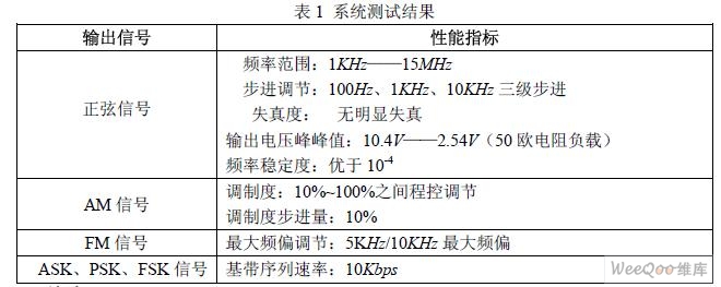
This paper adopts direct digital synthesis (DDS) technology, uses the dedicated integrated chip AD9834 as the sine wave generation module, and uses C8051F020 as the controller to complete the design of the entire system. The experimental results show that the output signal frequency is between 1 KHz and 15 MHz, and there is no obvious distortion. The output signal frequency can be adjusted in three levels: 100Hz, 1KHz, and 10KHz. Under a 50 ohm resistor load, the output voltage peak-to-peak value is between 2.35V and 10.45V. At the same time, the output of analog amplitude modulation signal (AM), analog frequency modulation signal (FM), binary amplitude shift keying signal (ASK), binary frequency shift keying signal (FSK) and binary phase shift keying signal (PSK) can be realized. The modulation degree of AM signal is adjusted in 10% steps. The maximum frequency deviation of FM signal is 5KHz/10KHz optional.
2 System Design
The overall block diagram of the system is shown in Figure 1. The system selects the integrated mixed signal C8051F020 microcontroller as the main controller, receives function selection, parameter setting and other information through the keyboard and display control chip 7279, and sends the output signal frequency and other information to the digital tube display in real time. At the same time, the controller converts the read key information into a control command and sends it to AD9834 through the serial interface. AD9834 generates sine signals, ASK, PSK, FSK and FM signals. The generation of AM signal is achieved by multiplying the output sine signal with a 1KHz biased sine signal, and the AM signal modulation degree is adjusted by adjusting the DC component.

2.1 Sine signal generation module
Direct digital synthesis (DDS) technology has many advantages such as high output signal accuracy, fast frequency conversion speed, continuous output signal, convenient control and high cost performance, so it is suitable for the design of high-frequency and high-precision sine signal generator. This system selects AD9834, and its working principle diagram is shown in Figure 2. It consists of a frequency word register, a phase word register, a phase accumulator, an adder, a sine ROM table and a DAC. Under the control clock signal, the accumulator accumulates the frequency word corresponding to the output signal frequency, and then adds it to the phase word to form the final phase information. The sine ROM table converts the phase information into amplitude information, and then the DAC generates a sine signal.
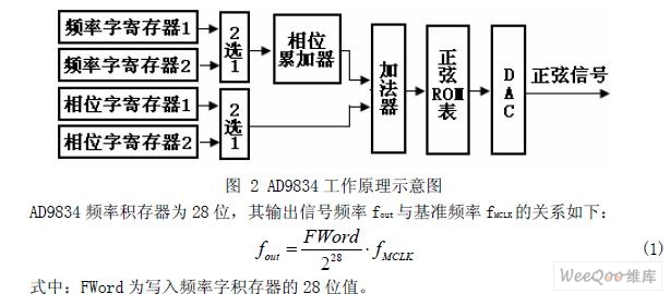
The frequency accuracy of the output signal is mainly determined by the accuracy of the reference frequency. In order to increase the amplitude of the AD9834 output signal, the high-frequency operational amplifier AD811 is used for signal amplification. However, considering the disadvantage that the amplitude of the output signal decreases as the frequency increases, the system uses a digital potentiometer X9C102 to achieve variable gain amplification, that is, the value of the digital potentiometer is changed according to the frequency of the output signal to change the gain [8]. The schematic diagram of the variable gain amplifier principle is shown in Figure 3.
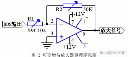
In the figure: R1 is the equivalent resistance value of the digital potentiometer X9C102.
2.2 Generation of PSK, FSK, and ASK signals
AD9834 has two phase word registers PHASE0 and PHASE1. The value in PHASE0 or PHASE1 can be selected as the initial phase word of the output signal through the off-chip pin PSELECT or the relevant bit of the on-chip control register. Based on this, write the values corresponding to 0 and π (000H and 800H) to PHASE0 and PHASE1 respectively, and the controller C8051F020 generates a 10kbps binary baseband sequence connected to port PSELECT, and the output end can get a binary PSK signal. [page]
Similarly, AD9834 has two frequency word registers FREQ0 and FREQ1, and the values in FREQ0 and FREQ1 can be selected as the frequency word of the output signal through the off-chip pin FSELECT or the relevant bits of the on-chip control register. Write the values corresponding to two different frequencies to FREQ0 and FREQ1 respectively, and the controller C8051F020 generates a 10kbps binary baseband sequence connected to port FSELECT, and the output end can get a binary FSK signal. The
generation method of ASK signal is similar to that of FSK, the only difference is that the value corresponding to 0Hz must be written into a frequency word register.
2.3 Generation of analog frequency modulation (FM) signal and analog amplitude modulation (AM) signal
This module uses a button to realize the selection of two-level program control with the maximum deviation frequency of 5KHz/10KHz. Use 8038 to generate a sine wave with a frequency of 1kHz and a peak-to-peak value of 2V as the modulation signal. According to the button information, it is determined whether it is a 5K deviation frequency or a 10K deviation frequency. Then the A/D of the single-chip microcomputer F020 collects the modulation signal, and uses formula 2 to convert the frequency into a digital quantity and write it into the frequency word register of AD9834, thereby realizing analog frequency modulation.

The sine signal with a frequency of 1kHz generated by 8038 is used as the modulation signal, and the D/A module of the controller C8051F020 generates a DC signal. The two signals are added to form a biased sine modulation signal. This signal and the sine signal (carrier) generated by AD9834 are multiplied by AD534 to generate an analog amplitude modulation wave. The modulation degree of the analog amplitude modulation signal can be changed by adjusting the size of the DC signal.
2.4 Key and display module
This module is implemented using the keyboard display management chip 7279. 7279 can automatically scan the key array and store the key information. The controller can read the key information through the serial interface, and can send the information to be displayed to 7279, which will automatically complete the scanning and display of the digital tube. This design simplifies the hardware connection and facilitates software processing.
2.5 System software design
The overall idea of system software design is: the controller reads the keyboard information, if a function key is pressed, the corresponding function program segment is executed according to the function selection; if an adjustment key is pressed, the signal output is paused until the parameters are set, and then the corresponding signal is output according to the function selection item.
3 Test results The final results of this system were experimentally measured, and the results are shown in Table 1:
4 Conclusion
This paper uses high-performance mixed signal C8051F020 microcontroller and DDS chip AD9834 to realize the design of high-frequency sinusoidal signal generator, which overcomes the shortcomings of the traditional method that the output signal is affected by the parameters of external components. At the same time, AD9834 has an internal integrated high-speed A/D, which can directly output sinusoidal signals, avoid external A/D, simplify the system hardware structure, and improve the system stability; based on the optional characteristics of AD9834 frequency word and phase word, the external part of the circuit can generate AM, FM, ASK, PSK, FSK and other modulation signals; AD9834 outputs sinusoidal signals with high accuracy, good stability, continuous output signals, and convenient control. Applying the signal generator based on the above advantages in engineering practice can improve the system cost performance and create good economic benefits. At the same time, the signal generator based on DDS technology will be widely used.
The author's innovation point is: using a multiplier to multiply the biased sinusoidal modulation signal with the carrier signal to generate an AM signal, and adjusting the magnitude of the DC component to adjust the AM signal modulation degree; collecting the modulation signal through A/D, and changing the output signal frequency according to the modulation signal amplitude information, thereby realizing the generation of FM signal.
Keywords:DDS
Reference address:Design of high frequency sine wave generator based on DDS technology
Sine signals are widely used and are usually used as standard signals for electronic performance experiments and parameter measurements. Therefore, the output waveform of the sine wave signal generator is required to have high accuracy, stability and low distortion. There are many ways to generate sine signals. You can use the function generator MAX038 or ICL8038 integrated chip to connect external discrete components to achieve this, and adjust the external capacitor or resistor to set the output signal frequency. However, the output signal is greatly affected by the parameters of the external discrete components, and the output signal frequency cannot be too high, and the frequency step adjustment cannot be achieved. In addition, the use of FPGA+D/A can realize the design of the sine signal generator and the frequency step adjustment, but when outputting high-frequency signals, high-speed D/A is required to work together.
This paper adopts direct digital synthesis (DDS) technology, uses the dedicated integrated chip AD9834 as the sine wave generation module, and uses C8051F020 as the controller to complete the design of the entire system. The experimental results show that the output signal frequency is between 1 KHz and 15 MHz, and there is no obvious distortion. The output signal frequency can be adjusted in three levels: 100Hz, 1KHz, and 10KHz. Under a 50 ohm resistor load, the output voltage peak-to-peak value is between 2.35V and 10.45V. At the same time, the output of analog amplitude modulation signal (AM), analog frequency modulation signal (FM), binary amplitude shift keying signal (ASK), binary frequency shift keying signal (FSK) and binary phase shift keying signal (PSK) can be realized. The modulation degree of AM signal is adjusted in 10% steps. The maximum frequency deviation of FM signal is 5KHz/10KHz optional.
2 System Design
The overall block diagram of the system is shown in Figure 1. The system selects the integrated mixed signal C8051F020 microcontroller as the main controller, receives function selection, parameter setting and other information through the keyboard and display control chip 7279, and sends the output signal frequency and other information to the digital tube display in real time. At the same time, the controller converts the read key information into a control command and sends it to AD9834 through the serial interface. AD9834 generates sine signals, ASK, PSK, FSK and FM signals. The generation of AM signal is achieved by multiplying the output sine signal with a 1KHz biased sine signal, and the AM signal modulation degree is adjusted by adjusting the DC component.

2.1 Sine signal generation module
Direct digital synthesis (DDS) technology has many advantages such as high output signal accuracy, fast frequency conversion speed, continuous output signal, convenient control and high cost performance, so it is suitable for the design of high-frequency and high-precision sine signal generator. This system selects AD9834, and its working principle diagram is shown in Figure 2. It consists of a frequency word register, a phase word register, a phase accumulator, an adder, a sine ROM table and a DAC. Under the control clock signal, the accumulator accumulates the frequency word corresponding to the output signal frequency, and then adds it to the phase word to form the final phase information. The sine ROM table converts the phase information into amplitude information, and then the DAC generates a sine signal.

The frequency accuracy of the output signal is mainly determined by the accuracy of the reference frequency. In order to increase the amplitude of the AD9834 output signal, the high-frequency operational amplifier AD811 is used for signal amplification. However, considering the disadvantage that the amplitude of the output signal decreases as the frequency increases, the system uses a digital potentiometer X9C102 to achieve variable gain amplification, that is, the value of the digital potentiometer is changed according to the frequency of the output signal to change the gain [8]. The schematic diagram of the variable gain amplifier principle is shown in Figure 3.

In the figure: R1 is the equivalent resistance value of the digital potentiometer X9C102.
2.2 Generation of PSK, FSK, and ASK signals
AD9834 has two phase word registers PHASE0 and PHASE1. The value in PHASE0 or PHASE1 can be selected as the initial phase word of the output signal through the off-chip pin PSELECT or the relevant bit of the on-chip control register. Based on this, write the values corresponding to 0 and π (000H and 800H) to PHASE0 and PHASE1 respectively, and the controller C8051F020 generates a 10kbps binary baseband sequence connected to port PSELECT, and the output end can get a binary PSK signal. [page]
Similarly, AD9834 has two frequency word registers FREQ0 and FREQ1, and the values in FREQ0 and FREQ1 can be selected as the frequency word of the output signal through the off-chip pin FSELECT or the relevant bits of the on-chip control register. Write the values corresponding to two different frequencies to FREQ0 and FREQ1 respectively, and the controller C8051F020 generates a 10kbps binary baseband sequence connected to port FSELECT, and the output end can get a binary FSK signal. The
generation method of ASK signal is similar to that of FSK, the only difference is that the value corresponding to 0Hz must be written into a frequency word register.
2.3 Generation of analog frequency modulation (FM) signal and analog amplitude modulation (AM) signal
This module uses a button to realize the selection of two-level program control with the maximum deviation frequency of 5KHz/10KHz. Use 8038 to generate a sine wave with a frequency of 1kHz and a peak-to-peak value of 2V as the modulation signal. According to the button information, it is determined whether it is a 5K deviation frequency or a 10K deviation frequency. Then the A/D of the single-chip microcomputer F020 collects the modulation signal, and uses formula 2 to convert the frequency into a digital quantity and write it into the frequency word register of AD9834, thereby realizing analog frequency modulation.

The sine signal with a frequency of 1kHz generated by 8038 is used as the modulation signal, and the D/A module of the controller C8051F020 generates a DC signal. The two signals are added to form a biased sine modulation signal. This signal and the sine signal (carrier) generated by AD9834 are multiplied by AD534 to generate an analog amplitude modulation wave. The modulation degree of the analog amplitude modulation signal can be changed by adjusting the size of the DC signal.
2.4 Key and display module
This module is implemented using the keyboard display management chip 7279. 7279 can automatically scan the key array and store the key information. The controller can read the key information through the serial interface, and can send the information to be displayed to 7279, which will automatically complete the scanning and display of the digital tube. This design simplifies the hardware connection and facilitates software processing.
2.5 System software design
The overall idea of system software design is: the controller reads the keyboard information, if a function key is pressed, the corresponding function program segment is executed according to the function selection; if an adjustment key is pressed, the signal output is paused until the parameters are set, and then the corresponding signal is output according to the function selection item.
3 Test results The final results of this system were experimentally measured, and the results are shown in Table 1:

4 Conclusion
This paper uses high-performance mixed signal C8051F020 microcontroller and DDS chip AD9834 to realize the design of high-frequency sinusoidal signal generator, which overcomes the shortcomings of the traditional method that the output signal is affected by the parameters of external components. At the same time, AD9834 has an internal integrated high-speed A/D, which can directly output sinusoidal signals, avoid external A/D, simplify the system hardware structure, and improve the system stability; based on the optional characteristics of AD9834 frequency word and phase word, the external part of the circuit can generate AM, FM, ASK, PSK, FSK and other modulation signals; AD9834 outputs sinusoidal signals with high accuracy, good stability, continuous output signals, and convenient control. Applying the signal generator based on the above advantages in engineering practice can improve the system cost performance and create good economic benefits. At the same time, the signal generator based on DDS technology will be widely used.
The author's innovation point is: using a multiplier to multiply the biased sinusoidal modulation signal with the carrier signal to generate an AM signal, and adjusting the magnitude of the DC component to adjust the AM signal modulation degree; collecting the modulation signal through A/D, and changing the output signal frequency according to the modulation signal amplitude information, thereby realizing the generation of FM signal.
Previous article:Design of Sine Signal Generator Based on Digital Frequency Synthesis DDS
Next article:Design of Digital Signal Generator Based on DSP and SOPC
- Popular Resources
- Popular amplifiers
Recommended Content
Latest Test Measurement Articles
- Keysight Technologies Helps Samsung Electronics Successfully Validate FiRa® 2.0 Safe Distance Measurement Test Case
- From probes to power supplies, Tektronix is leading the way in comprehensive innovation in power electronics testing
- Seizing the Opportunities in the Chinese Application Market: NI's Challenges and Answers
- Tektronix Launches Breakthrough Power Measurement Tools to Accelerate Innovation as Global Electrification Accelerates
- Not all oscilloscopes are created equal: Why ADCs and low noise floor matter
- Enable TekHSI high-speed interface function to accelerate the remote transmission of waveform data
- How to measure the quality of soft start thyristor
- How to use a multimeter to judge whether a soft starter is good or bad
- What are the advantages and disadvantages of non-contact temperature sensors?
MoreSelected Circuit Diagrams
MorePopular Articles
- LED chemical incompatibility test to see which chemicals LEDs can be used with
- Application of ARM9 hardware coprocessor on WinCE embedded motherboard
- What are the key points for selecting rotor flowmeter?
- LM317 high power charger circuit
- A brief analysis of Embest's application and development of embedded medical devices
- Single-phase RC protection circuit
- stm32 PVD programmable voltage monitor
- Introduction and measurement of edge trigger and level trigger of 51 single chip microcomputer
- Improved design of Linux system software shell protection technology
- What to do if the ABB robot protection device stops
MoreDaily News
- Allegro MicroSystems Introduces Advanced Magnetic and Inductive Position Sensing Solutions at Electronica 2024
- Car key in the left hand, liveness detection radar in the right hand, UWB is imperative for cars!
- After a decade of rapid development, domestic CIS has entered the market
- Aegis Dagger Battery + Thor EM-i Super Hybrid, Geely New Energy has thrown out two "king bombs"
- A brief discussion on functional safety - fault, error, and failure
- In the smart car 2.0 cycle, these core industry chains are facing major opportunities!
- The United States and Japan are developing new batteries. CATL faces challenges? How should China's new energy battery industry respond?
- Murata launches high-precision 6-axis inertial sensor for automobiles
- Ford patents pre-charge alarm to help save costs and respond to emergencies
- New real-time microcontroller system from Texas Instruments enables smarter processing in automotive and industrial applications
Guess you like
- ATE1133 audio decoding solution, USB sound card solution, TYPE C audio adapter chip solution
- What kind of LCD screen is suitable for use in a vibration environment
- Baobaobao~~~After the Chinese New Year, what new developments are there in the evaluation industry? Hurry up and take a look at the Evaluation Intelligence Bureau~
- [NUCLEO-L552ZE Review] Small thermometer
- STM3L4R5 driver for hts221 and stts751
- Cytech’s award-winning live broadcast: Let you learn about ADI’s digital health biosensor series live!
- Evaluation Weekly Report 20220406: Germany's PHYTEC's i.MX 8M+ AI board and RTT Renesas high-performance CPK-RA6M4 are here
- Is this post of the study club incomplete? The formula part?
- [NXP Rapid IoT Review] + Review the Bluetooth function and learn how to program the application
- I need help with a fully digital phase-locked loop Verilog code and modelsim simulation

 AWT-18046-30I


 京公网安备 11010802033920号