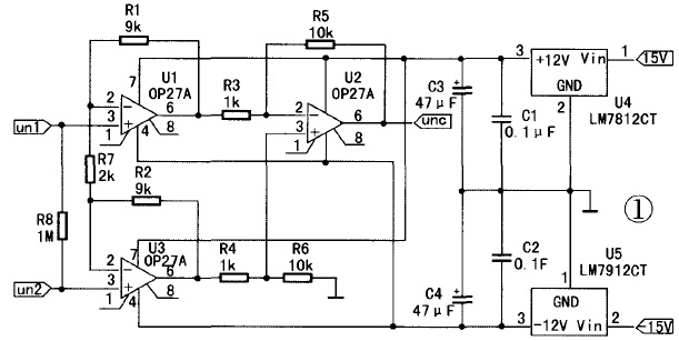
This instrumentation amplifier is composed of three OA27P integrated operational amplifiers. The characteristics of OA27P are low noise, high speed, low input offset voltage and excellent common mode rejection ratio. The instrumentation amplifier circuit is connected in the form of a proportional operational circuit, in which the first two operational amplifiers form the first stage, and both are connected in the form of in-phase input, so it has a very high input resistance. Due to the symmetric structure of the circuit, their drift and offset have the effect of canceling each other out. The latter operational amplifier forms a differential amplifier, which converts the differential input into a single-ended output. After calculation, the voltage gain of the instrumentation amplifier in this design is Au=R5/R3(1+2R1/R2)=100, and the result will be verified in the simulation.
The structural characteristics of the instrumentation amplifier: make the instrumentation amplifier an amplifier with high input resistance, high common mode rejection ratio, low offset voltage, offset current, noise and drift. When in use, the four resistors R4, R5, R6, and R7 in Figure 1 must be precise and matched, otherwise it will bring errors to the gain and reduce the common mode rejection ratio of the circuit.
1. Instrumentation amplifier circuit diagram
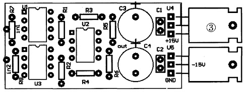
This design uses Prote199se circuit simulation software. After drawing the electrical schematic, the printed circuit board diagram can be automatically generated. Circuit simulation can also be performed. When drawing the electrical schematic, special attention should be paid to selecting the packaging form of various components. This is also one of the keys to whether the subsequent automatic wiring can be successful. The packaging forms of the components in this design are as follows: resistors (AXIAL0.3), electrolytic capacitors (RB.2/.4), ceramic capacitors (RAD0.1), integrated circuits (DIP-8), and three-terminal voltage regulators (TO-220).
The circuit diagram of the instrumentation amplifier is shown in Figure 1. R8 in the figure is added during the electrical inspection of the schematic diagram and does not need to be installed during actual production.
2. Drawing of electrical schematics and design of printed circuit boards
1. Enter the Prote199se SCH interface and draw the electrical schematic; After electrical inspection (Tool—ERC), the network table (Design—Great Netlist) can be generated after it is correct.
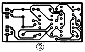
2. Enter the Prote199se PCB interface and draw the printed circuit board diagram. First determine the outer dimensions: 50mm long and 25mm wide. And the outer frame is required to be grounded and not closed as shown in Figure 2. Then load the network table (Design—Load Nets) and lay all the components reasonably on the printed circuit board. Set the automatic wiring parameters (Options—Rules). The most basic ones are line width, line spacing and number of layers. This design uses a single-sided board. After the parameters are set, you can execute the automatic wiring command (Auto Routs—All). Design results: Figure 2 is the printed circuit board diagram (scale: 1:1), and Figure 3 is the component distribution diagram (scale 2:1).
Three instrument amplifier circuit principle simulation
1. The simulation steps are as follows:
(1) Add simulation library
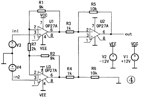
(2) Select and place the required components from the simulation component library. Connect the schematic diagram. Add the excitation source and set the parameters. As shown in Figure 4.
Note:
① R8, C1, C2, C3, C4, U4, and U5 can be disconnected;
② Set VCC to +15V and VEE to -15V;
③ VCC and VEE power supplies should be drawn separately.
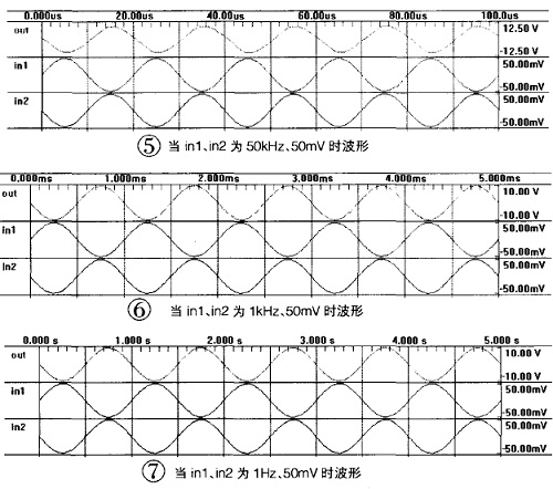
(3) Execute the Simulate—Setup command, add the signals input1, input2 and output to be analyzed, and then execute the Simulate—Run command. You can see the simulation waveforms you set. For example, Figure 5, Figure 6, and Figure 7.
2. Analysis of simulation results
(1) Output voltage Voul = 100 (Vin1 + Vin2);
(2) When the input signal frequency is about 50kHz, the output signal begins to distort;
(3) The low-frequency response of this instrument amplifier is very good. When the input signal frequency is 1Hz, the output signal is still not distorted.
Reference address:Instrumentation amplifier design and fabrication
The structural characteristics of the instrumentation amplifier: make the instrumentation amplifier an amplifier with high input resistance, high common mode rejection ratio, low offset voltage, offset current, noise and drift. When in use, the four resistors R4, R5, R6, and R7 in Figure 1 must be precise and matched, otherwise it will bring errors to the gain and reduce the common mode rejection ratio of the circuit.
1. Instrumentation amplifier circuit diagram
This design uses Prote199se circuit simulation software. After drawing the electrical schematic, the printed circuit board diagram can be automatically generated. Circuit simulation can also be performed. When drawing the electrical schematic, special attention should be paid to selecting the packaging form of various components. This is also one of the keys to whether the subsequent automatic wiring can be successful. The packaging forms of the components in this design are as follows: resistors (AXIAL0.3), electrolytic capacitors (RB.2/.4), ceramic capacitors (RAD0.1), integrated circuits (DIP-8), and three-terminal voltage regulators (TO-220).
The circuit diagram of the instrumentation amplifier is shown in Figure 1. R8 in the figure is added during the electrical inspection of the schematic diagram and does not need to be installed during actual production.

2. Drawing of electrical schematics and design of printed circuit boards
1. Enter the Prote199se SCH interface and draw the electrical schematic; After electrical inspection (Tool—ERC), the network table (Design—Great Netlist) can be generated after it is correct.
2. Enter the Prote199se PCB interface and draw the printed circuit board diagram. First determine the outer dimensions: 50mm long and 25mm wide. And the outer frame is required to be grounded and not closed as shown in Figure 2. Then load the network table (Design—Load Nets) and lay all the components reasonably on the printed circuit board. Set the automatic wiring parameters (Options—Rules). The most basic ones are line width, line spacing and number of layers. This design uses a single-sided board. After the parameters are set, you can execute the automatic wiring command (Auto Routs—All). Design results: Figure 2 is the printed circuit board diagram (scale: 1:1), and Figure 3 is the component distribution diagram (scale 2:1).


Three instrument amplifier circuit principle simulation
1. The simulation steps are as follows:
(1) Add simulation library
(2) Select and place the required components from the simulation component library. Connect the schematic diagram. Add the excitation source and set the parameters. As shown in Figure 4.

Note:
① R8, C1, C2, C3, C4, U4, and U5 can be disconnected;
② Set VCC to +15V and VEE to -15V;
③ VCC and VEE power supplies should be drawn separately.
(3) Execute the Simulate—Setup command, add the signals input1, input2 and output to be analyzed, and then execute the Simulate—Run command. You can see the simulation waveforms you set. For example, Figure 5, Figure 6, and Figure 7.

2. Analysis of simulation results
(1) Output voltage Voul = 100 (Vin1 + Vin2);
(2) When the input signal frequency is about 50kHz, the output signal begins to distort;
(3) The low-frequency response of this instrument amplifier is very good. When the input signal frequency is 1Hz, the output signal is still not distorted.
Previous article:Digital thermometer with memory function
Next article:Application of Digital Voltmeter ICL7106/7107
Recommended Content
Latest Test Measurement Articles
- Seizing the Opportunities in the Chinese Application Market: NI's Challenges and Answers
- Tektronix Launches Breakthrough Power Measurement Tools to Accelerate Innovation as Global Electrification Accelerates
- Not all oscilloscopes are created equal: Why ADCs and low noise floor matter
- Enable TekHSI high-speed interface function to accelerate the remote transmission of waveform data
- How to measure the quality of soft start thyristor
- How to use a multimeter to judge whether a soft starter is good or bad
- What are the advantages and disadvantages of non-contact temperature sensors?
- In what situations are non-contact temperature sensors widely used?
- How non-contact temperature sensors measure internal temperature
MoreSelected Circuit Diagrams
MorePopular Articles
- LED chemical incompatibility test to see which chemicals LEDs can be used with
- Application of ARM9 hardware coprocessor on WinCE embedded motherboard
- What are the key points for selecting rotor flowmeter?
- LM317 high power charger circuit
- A brief analysis of Embest's application and development of embedded medical devices
- Single-phase RC protection circuit
- stm32 PVD programmable voltage monitor
- Introduction and measurement of edge trigger and level trigger of 51 single chip microcomputer
- Improved design of Linux system software shell protection technology
- What to do if the ABB robot protection device stops
MoreDaily News
- CGD and Qorvo to jointly revolutionize motor control solutions
- CGD and Qorvo to jointly revolutionize motor control solutions
- Keysight Technologies FieldFox handheld analyzer with VDI spread spectrum module to achieve millimeter wave analysis function
- Infineon's PASCO2V15 XENSIV PAS CO2 5V Sensor Now Available at Mouser for Accurate CO2 Level Measurement
- Advanced gameplay, Harting takes your PCB board connection to a new level!
- Advanced gameplay, Harting takes your PCB board connection to a new level!
- A new chapter in Great Wall Motors R&D: solid-state battery technology leads the future
- Naxin Micro provides full-scenario GaN driver IC solutions
- Interpreting Huawei’s new solid-state battery patent, will it challenge CATL in 2030?
- Are pure electric/plug-in hybrid vehicles going crazy? A Chinese company has launched the world's first -40℃ dischargeable hybrid battery that is not afraid of cold
Guess you like
- 12. [Learning LPC1768 library functions] PWM experiment
- How to Actually Build a Drone
- What is the DMD lens action mechanism of the projector?
- Design of Watchdog Circuit Based on DSP Processor TMS320F2812
- Sitara AM335x issues
- Seeking long-term cooperation engineers to do part-time STM32 51 8S FPGA image processing
- 【K210 Series】6. Performance Test
- Capacitor selection problem after single-phase rectifier bridge
- Sensortile.box installation and testing
- How to start DSP c6678

 Operational Amplifier Stability Part 11


 京公网安备 11010802033920号