The realization of broadband impedance-controlled systems presents a formidable challenge to designers, manufacturers, and quality assurance managers of the central electronic building block, the printed circuit board (PCB). This challenge stems not from a lack of electromagnetic design knowledge, but from the enormous price pressure in the PCB industry: that is, the ideal radio frequency (RF) substrates that developers consider perfectly suited to clock rates in the GHz range are rarely used.
In contrast, low-cost FR4 materials with non-uniform dielectric constants (DC) across the substrate are often used. In addition, the lamination of core materials and prepregs into multilayer PCBs often results in geometrical non-uniformities, further adding to the sources of uncertainty. However, in order to meet the specified tolerances, many PCB manufacturers offer a service to check the line impedance, which in turn requires additional impedance test boards. These test boards are usually located at the edge of the PCB and therefore only partially represent the characteristics of the actual transmission lines of interest distributed across the entire production panel. In the worst case, the tested test board may be within the specified range, but the actual transmission line of interest does not meet the requirements.
Impedance fluctuations are often intolerable.
In addition to specific changes in materials and production processes, design parameter changes (such as layer changes, too short distances to the GND plane, PCB boundaries or other transmission lines) also occur from time to time, which ultimately lead to intolerable transmission line impedance fluctuations. The consequences of impedance fluctuations are clock edge degradation, intersymbol interference, unacceptable bit error rates, and ultimately performance degradation or even system failure.
The line impedance can be determined with high accuracy by time domain reflectometry (TDR). TDR technology has been used since the 1970s, mainly for detecting faults in underground or submarine cables. Figure 1 shows a block diagram of an impedance measurement device based on TDR technology. The TDR itself consists only of a voltage step generator and a broadband sampler with a data acquisition unit.

Figure 1: Block diagram of an impedance measurement system based on TDR technology.
The basic measurement principle is this: a voltage generator generates a step signal that is transmitted to the device under test (DUT) through adapters, cables and probes. When the interaction occurs along the entire length of the DUT, the signal will experience partial reflections and propagate back to the detector, thus achieving a spatial measurement of the DUT waveform impedance. Many people know this basic principle from radar applications, so TDR is often called cable radar.
The rise time tr of the step signal determines the spatial resolution and should be as short as possible (for the Sequid DTDR-65, tr ≈ 65ps, so the spatial resolution is about 5mm). Synchronization between the generator and the sampler (whose analog input bandwidth is at least 10GHz) is essential for low-noise operation (i.e. jitter values of only a few ps). It is ideal to use a "true through" sampler, without the need for external signal splitters or couplers. This benefit is obvious, because broadband signal splitters are usually resistive and increase insertion loss and noise. Finally, the TDR instrument also has a data recording unit, which is usually implemented with a microprocessor or FPGA.
High-frequency TDR devices do not normally use real-time sampling techniques, but rather sequential or random sampling techniques. Similar to stroboscopes, these devices can record rapidly changing periodic signals with reasonable technology. Data processing and visualization tasks are usually performed on a PC, which can be fully integrated in high-end instruments or connected via USB or Ethernet. The
adaptation of the measurement object to the TDR is a demanding task. For example, differential impedance measurements must use highly accurate phase-matched cables and probes. If this requirement is not met, even-mode and odd-mode conversions will reduce the measurement accuracy. In addition, the probe tip should be designed to match the impedance of the device under test to achieve the highest possible measurement accuracy.
Different systems on the market
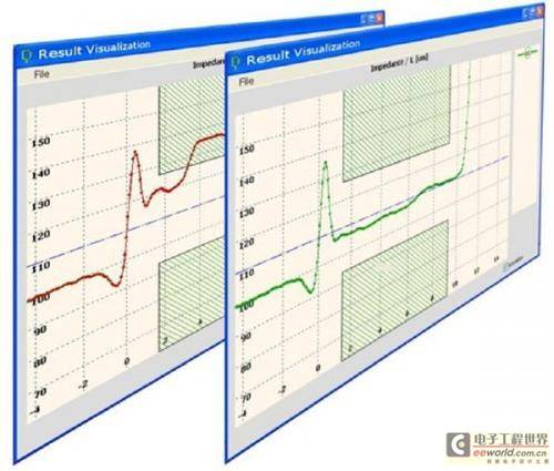
In the increasingly fast digital world, the measurement of line impedance has proven to be the most important TDR application today. Figure 2 shows examples of such spatially resolved measurements of a transmission line without interference (green curve) and with interference (red curve).

Figure 2: Reflection plots of RG 405 coaxial cable with a properly installed SMA connector (1, green) and an incorrectly installed SMA connector (2, red).
Only when all elements of the transmission path (not only the etched lines, but also the cables, connectors and even the terminating resistors in the integrated circuits) are impedance matched, is it possible to achieve reflection-free signal transmission between transmitter and receiver and thus the highest bit rates. Impedance control is therefore an important factor when evaluating the signal integrity of differential and single-ended lines.
Developers and manufacturers can choose from a large number of different types of differential TDR systems (DTDR) for impedance control: from very cost-effective systems to particularly expensive ones. Several well-known measurement technology manufacturers offer high-end TDR systems with high accuracy. These systems can be found in the field of high-speed oscilloscopes, generally combined with the necessary accessories such as (D)TDR probes. These devices are ideal for measuring transmission systems up to 20Gbit/s and beyond. However, impedance control seems to be a niche market for high-end equipment manufacturers. Therefore, they do not offer dedicated industrial solutions and potential users quickly get lost in the countless common RF measurement technologies before reaching the ultimate goal of "impedance measurement". In addition, due to their high performance and versatility, all these systems belong to the high price range, which makes the investment unattractive, especially if the TDR is not used continuously. [page]
Some TDRs with less commonality can be found in the field of industrial and special product measurement technology. Specific standard procedures have been established in these areas over the past two decades. These devices and the associated software are optimized for measuring the impedance of test boards and are deployed by many PCB manufacturers. However, these TDRs are not very suitable for the design and testing of random transmission lines inside PCBs because of the lack of suitable probes and - even worse - the too slow signal rise time tr leads to too small a signal bandwidth, which in turn only allows the characterization of lines with a minimum length of about 10 cm.
As a third version, there are also "self-made" solutions. There are a few very cost-effective (D)TDR devices on the market for this. In this way, the technical prerequisites are generally met by further purchasing components (TDR probes and phase adjustment cables). In this case, however, suitable software must be developed in terms of data recording, error reduction, impedance calculation and result archiving, so that solutions from one source can be traced back to the fact that they are not ultimately more cost-effective and safe.
Sequid GmbH originally developed high-resolution and high-precision TDR systems for judging the quality of fish meat. In cooperation with the German PCB manufacturer Elekonta Marek GmbH, the existing basic technology was further developed into a very high-performance system (Sequid DTDR-65) that meets all requirements for impedance-controlled measurements. This is a highly stable differential time domain reflectometer suitable for impedance measurements of differential and single-ended transmission lines at rates up to 10Gbit/s. The instrument has a 65ps step signal generator and thus supports high-resolution measurements on test boards and actual circuits. In addition, the DTDR-65 has particularly good jitter performance (Jrms < 500fs), which is usually only available in high-end devices.
A software solution was developed that enables impedance measurements to be performed by non-RF experts. This solution includes not only basic functions (such as device control) but also intuitive and actionable functions for displaying the line impedance. Tolerance templates make it easy to make a PASS/FAIL statement. Some simple application examples are described below.
Figure 3 shows the reflection diagram of an RG 405 coaxial cable, where the coaxial cable is assembled with SMA connectors according to the assembly specification (1) and not according to the assembly specification (2). The line impedance Z0 ≈ 51.5Ω for both RG 405 cables, with a very clear transition in the connector area. In the case of incorrectly installed connectors, a drop in capacitance (deformation towards lower impedance) is visible. This effect frequently occurs when the outer and inner conductors are installed too close together (i.e. a capacitor is built up).

Figure 3: Reflection plots of RG 405 coaxial cable with a correctly installed SMA connector (1, green) and an incorrectly installed SMA connector (2, red).
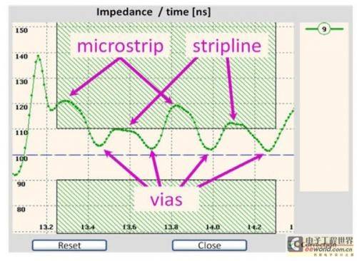
Figure 4 shows the impedance curve of the differential transmission line on a 4-layer printed test circuit. The transmission path starts as a microstrip line in the first layer (top layer), then goes to the second layer through a via, where it is still a microstrip line, and then returns to the surface of the first layer through a second via. This route is repeated several times and finally terminates on the first layer. Obviously, this test circuit cannot achieve the target impedance of 100Ω: the characteristic impedance of the microstrip line and stripline are Z0≈120Ω and Z0≈110Ω respectively. It can be clearly seen from this figure that the capacitance factor of the via will seriously affect the signal integrity in the actual system, especially at high data rates.

Figure 4: Reflection plot of differential lines routed on two different layers of an FR4 substrate.
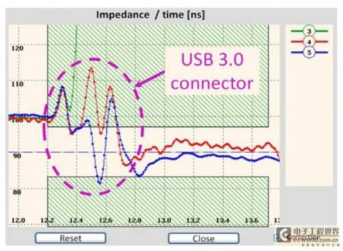
As a final example, Figure 5 shows the reflection plots of a USB 3.0 connector and cable. The nominal impedance of the USB 3.0 assembly is Z0 = 90Ω ± 7Ω. The TDR device was still operated on a reference impedance of 100Ω (time range t < 12.2ns). The first reflection caused by the transition from the test adapter to the USB 3.0 connector occurs at about 12.3ns, as expected and consistent with all measurements. Curve 3 (green) represents the result of an open adapter, where the fast impedance rise indicates the (high impedance) end of the adapter. Curves 4 and 5 (red and blue) represent two different USB 3.0 cable assemblies, each consisting of an adapter and a subsequent cable. While the cables are within the specification, the adapters do not. In particular, the red curve shows a maximum impedance of about 122Ω, which produces severe reflections that could cause the USB 3.0 controller to reduce the data rate.
In summary, all examples clearly show that developers can use the DTDR-65 to gain intuitive insights into the transmission path. The task of developers and quality inspectors often includes the easy-to-understand documentation of the results obtained. This task is important but unfortunately very time-consuming and tedious. However, this unwelcome task can now be greatly simplified with the built-in automated report generation tool, which generates graphical and statistical extensive evaluation results in just a few clicks. In addition, online impedance calculators are available for the most common line types.

Figure 5: Reflection plots of a USB 3.0 adapter with an open circuit (3) and two different USB 3.0 cable assemblies (4 and 5).
The necessary accessories
include high-quality phase-adjusted coaxial cables and TDR probes for different types of applications: industrial probes for serial measurements in production and high-precision probes for research and development - see Figure 6. The DTDR-65 also has excellent electromagnetic shielding performance and can be used in battery-powered mobile applications.

Figure 6: Different probes and accessories for the DTDR-65 time domain reflectometer.
Previous article:Influencing factors that should be considered in the use of gas ultrasonic flowmeter
Next article:Design of MRS signal acquisition module based on orthogonal vector amplification ---- Acquisition module software implementation
Recommended ReadingLatest update time:2024-11-16 20:50


- Keysight Technologies Helps Samsung Electronics Successfully Validate FiRa® 2.0 Safe Distance Measurement Test Case
- From probes to power supplies, Tektronix is leading the way in comprehensive innovation in power electronics testing
- Seizing the Opportunities in the Chinese Application Market: NI's Challenges and Answers
- Tektronix Launches Breakthrough Power Measurement Tools to Accelerate Innovation as Global Electrification Accelerates
- Not all oscilloscopes are created equal: Why ADCs and low noise floor matter
- Enable TekHSI high-speed interface function to accelerate the remote transmission of waveform data
- How to measure the quality of soft start thyristor
- How to use a multimeter to judge whether a soft starter is good or bad
- What are the advantages and disadvantages of non-contact temperature sensors?
- Innolux's intelligent steer-by-wire solution makes cars smarter and safer
- 8051 MCU - Parity Check
- How to efficiently balance the sensitivity of tactile sensing interfaces
- What should I do if the servo motor shakes? What causes the servo motor to shake quickly?
- 【Brushless Motor】Analysis of three-phase BLDC motor and sharing of two popular development boards
- Midea Industrial Technology's subsidiaries Clou Electronics and Hekang New Energy jointly appeared at the Munich Battery Energy Storage Exhibition and Solar Energy Exhibition
- Guoxin Sichen | Application of ferroelectric memory PB85RS2MC in power battery management, with a capacity of 2M
- Analysis of common faults of frequency converter
- In a head-on competition with Qualcomm, what kind of cockpit products has Intel come up with?
- Dalian Rongke's all-vanadium liquid flow battery energy storage equipment industrialization project has entered the sprint stage before production
- Allegro MicroSystems Introduces Advanced Magnetic and Inductive Position Sensing Solutions at Electronica 2024
- Car key in the left hand, liveness detection radar in the right hand, UWB is imperative for cars!
- After a decade of rapid development, domestic CIS has entered the market
- Aegis Dagger Battery + Thor EM-i Super Hybrid, Geely New Energy has thrown out two "king bombs"
- A brief discussion on functional safety - fault, error, and failure
- In the smart car 2.0 cycle, these core industry chains are facing major opportunities!
- The United States and Japan are developing new batteries. CATL faces challenges? How should China's new energy battery industry respond?
- Murata launches high-precision 6-axis inertial sensor for automobiles
- Ford patents pre-charge alarm to help save costs and respond to emergencies
- New real-time microcontroller system from Texas Instruments enables smarter processing in automotive and industrial applications
- Transformer noise
- The circuit board failed the EMC certification, and the signal is unstable! Why can I just add a small return capacitor?
- Uninstall and reinstall IAR EM8051
- Doherty Amplifier
- Three points are destined?
- How to increase the current of RLC oscillation circuit
- EEWORLD University----[High Precision Laboratory] Motor Drive: Stepper Motor Driver
- 2812 TxPR register write failure caused by TxCON highest bit
- (Transfer) CC2640R2F BLE5.0 Bluetooth protocol stack Generic Attribute Profile (GATT)
- [GD32L233C-START Evaluation] Development Environment Construction

 Modern Electronic Technology Training Course (Edited by Yao Youfeng)
 Pad loss problem when exporting GERBER from PADS
 2024 DigiKey Innovation Contest


 京公网安备 11010802033920号