Chapter 3 High-resistance device noise test technology
3.1 Analysis of noise test problems of high impedance samples
Researchers have found that when the study of noise is expanded to high-resistance devices or high-resistance materials such as capacitors, MOS device gate oxide layers, and high-resistance resistors, traditional noise testing techniques are no longer effective, and many new technical problems and challenges emerge.
(1) High source impedance attenuates voltage noise signals
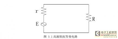
The traditional test method of testing voltage noise cannot fully amplify the signal. When the input impedance of the amplifier is fixed, the excessive resistance of the test sample will cause the weak noise signal to not be fully amplified, affecting signal extraction. See the figure below for details;
r is the signal source impedance, R is the amplifier input impedance, which is usually in the range of tens of MΩ to hundreds of MΩ or even GΩ, and E is the noise signal. According to Ohm's law, when the r value is not large, that is, the sample being measured is a medium-impedance sample, the noise signal voltage almost entirely falls on the amplifier input impedance, and the signal is captured by the amplifier without attenuation. However, when the size of r reaches a range comparable to R or even a range larger than R, the signal voltage falling on R will become a fraction or even one percent of E. Since the noise signal voltage is originally a weak signal, a fraction or even one percent of its value will become even weaker, even reaching an order of magnitude comparable to the background noise. Coupled with the limited accuracy of the data acquisition card, this will affect the signal extraction accuracy during the subsequent analog-to-digital conversion of the signal.
(2) High bias voltage conditions will reduce the life of the coupling capacitor and even cause the coupling capacitor to break down.
When the device resistance is too high, if the traditional method of measuring voltage noise is used, it may be necessary to add a large DC bias voltage across the device to stimulate obvious and measurable low-frequency noise. This will result in the following two limitations in the test conditions: first, the amplifier cannot use DC coupling when collecting signals, which will result in the inability to measure very low-frequency signals; second, even if AC coupling is used, the voltage drop on the coupling capacitor is too high, which may exceed the rated voltage of the capacitor and break down the capacitor; excessive voltage will also affect the life of the coupling capacitor.
(3) The bandwidth of the current noise signal is too narrow. The test circuit for MOS gate oxide leakage current noise abroad is shown in Figure 3.2. This method measures the current noise by applying a certain bias voltage on the gate oxide layer.
The bias stage in the lower part of Figure 3.2 is a typical active filter, which is used to filter out AC interference from the DC source to ensure that the test results only contain the noise signal of the test sample. The DUT in the upper part of Figure 3.2 is the sample to be tested. The amplifier circuit based on TLC070 is built into a transimpedance amplifier mode to convert the gate leakage current signal into a proportional voltage signal.
The test method in Figure 3.2 has the problem of too narrow signal passband. Since the current noise of high-resistance devices under the same bias voltage will be very weak, the amplification factor is usually set very large, which leads to a lower bandwidth when the amplifier bandwidth-gain product is constant. This can be seen from the relationship between the bandwidth and gain of SR570 in Figure 3.3.
(4) The high frequency of capacitor leakage current noise is attenuated
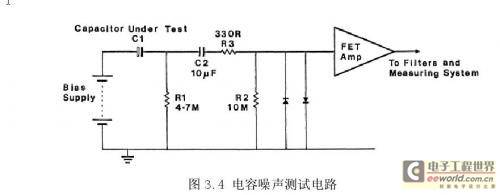
The schematic diagram of the existing testing technology for capacitors is shown in Figure 3.4:
The noise leakage current flowing through the capacitor C1 to be tested will generate a noise voltage drop on R1. The amplifier tests the noise voltage signal on R1. R1 uses a large-value winding resistor, but relative to the amplifier, R1 is equivalent to a low source impedance, so the signal will not be attenuated, and because R1 is considered to be noise-free, the noise signal from R1 is the noise signal of C1. [page]
The method in Figure 3.4 has the following problem: Since R l and C 1 form a low-pass filter network, when the angular frequency ω ≥ 1/ R 1 C 1 , the signal will be attenuated due to the existence of the filter network, forming the spectrum diagram shown in the following figure:
It can be seen that the signal starts to decay severely from 200Hz. Even if the amplifier gain is small or the frequency band is large, the attenuation cannot be changed. This shows that the serious defect of this method is that it is also impossible to observe the spectrum image of higher frequencies.
(5) The symmetrical potential test method cannot measure a single device.
The schematic diagram of the existing noise test technology for high-resistance resistors is shown in the figure above. RD is the resistor to be tested. The circuit measures the noise of two resistors RD at a time and is powered by two batteries with the same voltage value. J1 is a first-stage amplifier. From the circuit structure, we can see that theoretically the voltage across the two resistors can be infinite. This is because the input of J1 is always kept at a potential close to zero volts and will not saturate the amplifier.
The symmetrical potential test method in Figure 3.6 has the following disadvantages: First, one of its serious defects is that it cannot measure the noise of a single device; second, it requires that the impedance of the two samples is completely equal. For resistors with particularly large resistance values, due to their limited process accuracy, it is extremely difficult to achieve the ideal situation that the resistance of the two test samples is equal.
(6) The noise of the multi-stage amplifier is too large
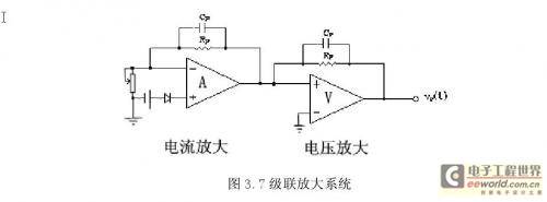
In order to alleviate the problem of the current amplifier's narrow bandwidth, some researchers have used a multi-stage amplification method [6], which can achieve the effect of widening the bandwidth, as shown in Figure 3.7. This method uses the current amplifier as the first stage of amplification and appropriately reduces the amplification factor of the first stage, thereby widening the signal passband. The reduced amplification factor of the first stage is compensated by the second stage voltage amplifier, thereby ensuring that the passband of the noise signal is widened without reducing the overall amplification factor. Although this method can widen the bandwidth, it does so at the expense of increasing the system background noise, thereby reducing the test accuracy. This phenomenon can be seen in the figure below:

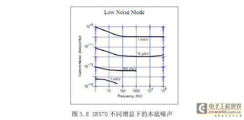
The figure above shows the relationship between the background noise and the amplification factor of the SR570 transimpedance amplifier. It can be clearly seen that when the amplification factor is reduced, the background noise of the system will increase significantly, which seriously limits the accuracy of the test system. Such a test system is difficult to measure low noise. Through actual testing, we found that in most tests, the background noise of the secondary amplifier circuit is much larger than the signal to be tested and cannot be used.
Previous article:Research on low-frequency noise test technology and application of high-resistance devices--Solution for noise test of high-resistance samples
Next article:Research on low-frequency noise test technology and application of high-resistance devices--theory of low-frequency noise test technology (I)
Recommended ReadingLatest update time:2024-11-16 14:27

- Keysight Technologies Helps Samsung Electronics Successfully Validate FiRa® 2.0 Safe Distance Measurement Test Case
- From probes to power supplies, Tektronix is leading the way in comprehensive innovation in power electronics testing
- Seizing the Opportunities in the Chinese Application Market: NI's Challenges and Answers
- Tektronix Launches Breakthrough Power Measurement Tools to Accelerate Innovation as Global Electrification Accelerates
- Not all oscilloscopes are created equal: Why ADCs and low noise floor matter
- Enable TekHSI high-speed interface function to accelerate the remote transmission of waveform data
- How to measure the quality of soft start thyristor
- How to use a multimeter to judge whether a soft starter is good or bad
- What are the advantages and disadvantages of non-contact temperature sensors?
- Innolux's intelligent steer-by-wire solution makes cars smarter and safer
- 8051 MCU - Parity Check
- How to efficiently balance the sensitivity of tactile sensing interfaces
- What should I do if the servo motor shakes? What causes the servo motor to shake quickly?
- 【Brushless Motor】Analysis of three-phase BLDC motor and sharing of two popular development boards
- Midea Industrial Technology's subsidiaries Clou Electronics and Hekang New Energy jointly appeared at the Munich Battery Energy Storage Exhibition and Solar Energy Exhibition
- Guoxin Sichen | Application of ferroelectric memory PB85RS2MC in power battery management, with a capacity of 2M
- Analysis of common faults of frequency converter
- In a head-on competition with Qualcomm, what kind of cockpit products has Intel come up with?
- Dalian Rongke's all-vanadium liquid flow battery energy storage equipment industrialization project has entered the sprint stage before production
- Allegro MicroSystems Introduces Advanced Magnetic and Inductive Position Sensing Solutions at Electronica 2024
- Car key in the left hand, liveness detection radar in the right hand, UWB is imperative for cars!
- After a decade of rapid development, domestic CIS has entered the market
- Aegis Dagger Battery + Thor EM-i Super Hybrid, Geely New Energy has thrown out two "king bombs"
- A brief discussion on functional safety - fault, error, and failure
- In the smart car 2.0 cycle, these core industry chains are facing major opportunities!
- The United States and Japan are developing new batteries. CATL faces challenges? How should China's new energy battery industry respond?
- Murata launches high-precision 6-axis inertial sensor for automobiles
- Ford patents pre-charge alarm to help save costs and respond to emergencies
- New real-time microcontroller system from Texas Instruments enables smarter processing in automotive and industrial applications
- [ufun learning] Practical Part 1: "PWM control of DC motor acceleration, deceleration, forward and reverse rotation"
- Usage of CC6678 Digital Signal Processor (DSP)
- ZigBee On Windows Mobile--ZigBee Module Antenna Design
- Help, has anyone encountered this problem using the Pickit 3 Programmer programming tool?
- D Question Development
- "Linux Shell Programming from Beginner to Mastery"——Embedded Linux learning resources are free!
- Design of intelligent charging lighting control system based on MSP430 single chip microcomputer
- GD32E231 DIY Contest (2) GD32E231C Development Environment Getting Started DEMO Test
- [NXP Rapid IoT Review] A Bluetooth BLE communication app designed for NXP IoT in the third week
- Lithium-ion battery SOC state of charge measurement


 Real-time driver monitoring system via modal and viewpoint analysis
 CVPR 2023 Paper Summary: Robotics


 京公网安备 11010802033920号