The resistance strain sensor is a sensor that uses the resistance strain effect of metal to measure small changes. The strain sensor is a sensor based on measuring the strain generated by the force deformation of an object. The resistance strain gauge is the core part of the resistance strain sensor and directly affects various performance indicators of the sensor. The working principle of the resistance strain gauge is the strain effect of metal. The phenomenon that the resistance of a metal conductor changes with the size of the mechanical deformation it is subjected to is called the resistance strain effect of metal.
In the existing aircraft strength test, the measurement principle of resistance strain gauge is generally adopted. A resistance strain gauge is pasted on each strength assessment point. When conducting the test, the strength of the aircraft body node is obtained by reading the strain value. Ordinary aircraft use about 6,000 to 12,000 strain gauges per aircraft, and large aircraft will have more. Each strain gauge has 3 electrical wires, so there are tens of thousands of wires in total, which occupies a large area, has complicated wiring, and the lines are seriously entangled, causing chaos on the test site. Once a strain gauge has a problem, it will be very difficult to find it on site, which greatly increases the complexity and cycle of strength testing.
This paper uses optical fiber to transmit strain signals. With modular design, the number of strain gauges that can be collected increases exponentially through cascading between modules. Tens of thousands of electrical signals are converted into one or several optical signals for transmission. There is only one optical cable from the test site to the monitoring room.
Moreover, due to the modular design, if a signal has a problem, it can be directly replaced with a live plug-in, which greatly shortens the cycle of finding the source of the problem during the monitoring process. The introduction of optical fiber technology promotes the reliability and structural optimization of the aircraft strength monitoring system.
1 System Design
1.1 Structural design
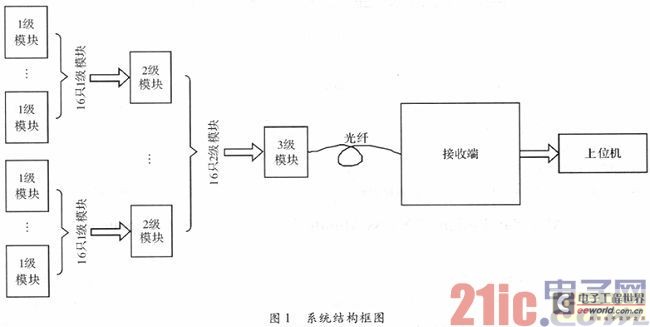
The system structure is shown in Figure 1. The components are divided into three parts: the transmitter, the optical fiber, and the receiver. The transmitter consists of a level 1 module, a level 2 module, and a level 3 module. The level 1 module is used to collect strain signals. Each level 1 module can collect up to 16 strain signals; the level 2 module and the level 3 module are used for data multiplexing and communication. Each level 2 module can connect up to 16 level 1 modules and can collect up to 256 strain signals; each level 3 module can connect up to 16 level 2 modules and can collect up to 4,096 strain signals. An aircraft only needs up to 3 level 3 modules to achieve the purpose of collecting all nodes. The level 3 module converts the collected 4,096 stress signals into optical signals and transmits them to the remote end through optical fiber. At the remote end, it is converted into electrical signals through photoelectric conversion and received, decoded, extracted, and sent to the host computer for processing. Moreover, this product can increase or decrease the number of modules according to the number of strain channels to be collected. If hundreds of strain signals are to be collected, only several level 1 and level 2 modules are needed. If dozens of strain signals are to be collected, several level 1 modules can meet the requirements and can be combined freely. If one of the modules does not work properly, it can be replaced directly without affecting the operation of the entire system.
1.2 Component Design
The 16 strain signals are converted into mV-level voltage signals through the Wheatstone bridge and sent to the strain signal conditioning circuit for linear amplification and filtering. The multiplexer selects one of the 16 channels and sends it to a high-precision A/D converter with an accuracy of 24 bits to digitize the analog signal. The CPLD receives the digital signal from the A/D and then sends a command to the multiplexer to switch to the next strain signal to continue collecting. The cycle continues in sequence, and all 16 strain signals are collected directly to complete an acquisition cycle. The CPLD converts the collected 16 strain signals into serial signals and sends them to the data transmission unit for data transmission processing and sends them to the next level module. The schematic block diagram of the level 1 module is shown in Figure 2.

There are the following difficulties in detecting weak signals: (1) Fluctuations in the bridge voltage cause fluctuations in the output. (2) The poor consistency of the strain gauge resistance causes measurement errors. (3) The strain gauge has an inaccurate output due to the lack of temperature compensation. (4) The number of bits of the A/D converter affects the accuracy of the conversion and the speed is low. Conversely, the conversion accuracy is low and the speed is high. (5) The accuracy of the filter design will determine whether the noise signal can be filtered out. (6) When the cantilever arm starts to suspend the weight, the output voltage will be unstable, resulting in errors.
In response to the above problems, the improvement methods proposed in this paper are as follows: (1) Use a high-precision voltage-stabilized power supply. (2) Screen the strain gauges and use strain gauges with the same physical properties. (3) Use a temperature compensation device for the strain gauges and compensate them in the software to minimize the impact of temperature on the strain gauges. (4) Increase the number of bits of the A/D converter as much as possible while meeting the rate performance indicators to reduce the quantization error. (5) Further accurately design the filter to fully filter out the noise signal. (6) Delay for a certain period of time and wait for the signal to stabilize before sampling.
16 channels of serial data are sent to the second-level module. CPLD receives the 16 channels of serial signals. Because each serial signal contains 16 channels of strain signals, the 16 channels of serial signals contain a total of 256 channels of strain data. CPLD processes the 256 channels of strain data by data multiplexing, data encoding, parallel-to-serial conversion, etc., converts them into serial signals arranged in a certain number of times, and sends them to the next-level module. The principle block diagram of the second-level module is shown in Figure 3.
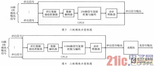
The principle block diagram of the 3-level module is shown in Figure 4. The principle of the 3-level module is the same as that of the 2-level module. It receives 16 strain signals sent by the 2-level module, a total of 4,096 strain signals, which are then converted into optical signals through optical modules and sent to the remote end through optical fibers, where they are received by the receiving end.
The principle block diagram of the receiving end is shown in Figure 5. The receiving end receives the optical signal sent from the remote end by the optical module, converts it into an electrical signal and sends it to the subsequent circuit for data reception, decoding and other processing. It receives 4096 strain signals and then arranges them in sequence according to the number of data placements required by the host computer. The communication interface chip sends the strain data to the host computer for storage, processing and display of the strain signal.

2. Selection of main components
2.1 ADC converter selection
For ADC converters, the selection criteria mainly depend on sampling frequency and bit number, as well as price, delivery cycle, application and other factors. Since the system has many channels of analog signals, a multi-channel A/D needs to be selected. The system uses AD7490 from AD. AD7490 is a 12-bit high-speed, low-power analog-to-digital converter with an input signal of up to 1 MHz, 16 channels, and a single power supply of 2.7 to 5.25 V. The sampling rate can reach 1 MSample·s-1, and the operating frequency can reach 20 MHz at a working voltage of 5 V. The communication interface is a high-speed serial interface SPI. [page]
2.2 CPLD Selection
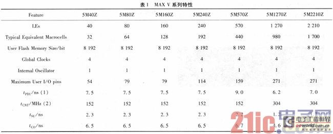
Altera's MAX V series CPLD has the characteristics of low voltage and low consumption. The characteristics of the MAX V series are shown in Table 1. According to actual needs, 5M570Z is selected as the control core of the product.
3 Simulation Results
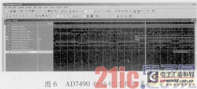
Through data acquisition function simulation, that is, AD7490 controller driver simulation. It is verified that the code design meets the design function. The specific process is as follows: The analog-to-digital conversion chip AD7490 needs to be initialized before normal operation, and there are 3 DUMMY cycles. The AD7490 write cycle includes 16 ADC clocks, which are obtained by dividing the system clock. The ADC working clock is set to 10 MHz and the system clock is set to 20 MHz.
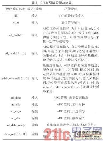
The CPLD pin assignment is shown in Table 2.
The initialization result of AD7490 is shown in Figure 6. As can be seen from Figure 6, after the system clock is valid, AD7490 first performs 3 initialization cycles, and then performs mode setting and acquisition operations as needed.
After AD7490 is initialized, data acquisition will be performed. The 16-channel AD7490 is divided into three acquisition modes, namely 00 mode, 01 mode and 11 mode. The design adopts mode, and all three modes are simulated. ad_mode is the mode selection input pin. The simulation results are shown in Figure 7.
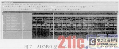
As shown in Figure 7, after initialization, AD7490 selects three modes in turn for simulation, and the verification results are correct and meet the design requirements.
4 Conclusion
A strain signal acquisition system was designed using A/D+CPLD for use in aircraft strength monitoring tests. Optical fiber was used as the transmission medium for long-distance transmission. The following conclusions were drawn:
(1) The system schematic design and PCB drawing were completed, and the system hardware circuit board was made. After the hardware system debugging, the hardware part met the design requirements and realized the connection function between each module.
(2) CPLD adopts a top-down design concept, starting from the top-level system structure block diagram, and divides the system into ADC control module, data processing module, and communication module. From the simulation and testing of each sub-module in the design, it can be seen that the software implementation meets the system design requirements, and the CPLD chip plays the role of the main controller. The data of the entire system is stable during data acquisition, transmission, storage, and transmission.
(3) In the software design part, the basic principles and hardware principles of CPLD design are followed, and common design techniques are used, such as calling dual-port RAM for ping-pong operations, serial-to-parallel conversion, and pipeline operations, so as to avoid data overflow during the acquisition or transmission process. Competition and risk in the timing logic lead to data loss. Handling the timing relationship well is the key to high-speed acquisition systems. Timing constraints are added to each different module in the design to meet the timing convergence after comprehensive layout and routing, and to handle the delay processing of critical paths.
Previous article:Analyze the technical standards of cables and connectors and grasp the key points of certification testing
Next article:Source measurement unit instruments equipped with capacitive touch screens significantly improve work efficiency
- Popular Resources
- Popular amplifiers
- Seizing the Opportunities in the Chinese Application Market: NI's Challenges and Answers
- Tektronix Launches Breakthrough Power Measurement Tools to Accelerate Innovation as Global Electrification Accelerates
- Not all oscilloscopes are created equal: Why ADCs and low noise floor matter
- Enable TekHSI high-speed interface function to accelerate the remote transmission of waveform data
- How to measure the quality of soft start thyristor
- How to use a multimeter to judge whether a soft starter is good or bad
- What are the advantages and disadvantages of non-contact temperature sensors?
- In what situations are non-contact temperature sensors widely used?
- How non-contact temperature sensors measure internal temperature
- LED chemical incompatibility test to see which chemicals LEDs can be used with
- Application of ARM9 hardware coprocessor on WinCE embedded motherboard
- What are the key points for selecting rotor flowmeter?
- LM317 high power charger circuit
- A brief analysis of Embest's application and development of embedded medical devices
- Single-phase RC protection circuit
- stm32 PVD programmable voltage monitor
- Introduction and measurement of edge trigger and level trigger of 51 single chip microcomputer
- Improved design of Linux system software shell protection technology
- What to do if the ABB robot protection device stops
- CGD and Qorvo to jointly revolutionize motor control solutions
- CGD and Qorvo to jointly revolutionize motor control solutions
- Keysight Technologies FieldFox handheld analyzer with VDI spread spectrum module to achieve millimeter wave analysis function
- Infineon's PASCO2V15 XENSIV PAS CO2 5V Sensor Now Available at Mouser for Accurate CO2 Level Measurement
- Advanced gameplay, Harting takes your PCB board connection to a new level!
- Advanced gameplay, Harting takes your PCB board connection to a new level!
- A new chapter in Great Wall Motors R&D: solid-state battery technology leads the future
- Naxin Micro provides full-scenario GaN driver IC solutions
- Interpreting Huawei’s new solid-state battery patent, will it challenge CATL in 2030?
- Are pure electric/plug-in hybrid vehicles going crazy? A Chinese company has launched the world's first -40℃ dischargeable hybrid battery that is not afraid of cold
- Has anyone used ST's vl53l0x laser distance sensor?
- Simple use of window function in Matlab
- I want a vhdl written eeprom read and write function, power failure data will not be lost
- How to measure the output ripple of a single-phase inverter with an oscilloscope
- No color difference splicing screen
- Analysis of optimization methods for overcrowded solder joints in PCB design
- FPGA design clean code is a core skill for programmers
- Toshiba DC motors and stepper motors make your motors smarter!
- Xilinx Vivado Quick Start - HDL Flow - Contains videos, projects and Chinese version documents
- Temperature problems solved for you (I) Basic principles of temperature sensing

 TC52N4143ECTRT


 京公网安备 11010802033920号