In the field of electronic technology, oscilloscopes are widely used. They can be used to observe the full picture of the signal and measure the basic parameters of the signal, such as amplitude, frequency, and period. The afterglow time of the fluorescent material used in the traditional analog oscilloscope is fixed, which makes it difficult to observe signals with longer periods. In addition, analog oscilloscopes cannot perform some special mathematical processing on the signal (such as FFT). The digital oscilloscope can overcome the shortcomings of the analog oscilloscope. It uses various advanced measurement technologies to meet various applications. For example, based on the sampling principle, a high-speed A/D converter is used to realize high-speed data acquisition, digitize the analog signal, and then use the powerful data processing capability of the processor to realize various digital signal processing algorithms, display the waveform intuitively in a graphical way, and obtain various rich parameters of the measured signal.
1 System Overall Plan
The system block diagram of this design is shown in Figure 1. Thanks to the flexibility of FPGA, most of the system functions are completed inside the FPGA, making the overall structure very simple. The peripheral circuit mainly includes A/D conversion module, LCD display, SD card, FLASH and buttons. The function of the A/D conversion module is to realize the conversion of analog signals to digital signals; the function of the FLASH module is to store the firmware program of the SoPC (System-on-a-Programmable-Chip) system-on-chip; the function of the SD card module is to realize long-term and large-scale storage of measurement information and provide an interface with the PC to facilitate later analysis on the computer; the function of the LCD module is to display the measurement signal waveform and related parameters in real time; the function of the button module is to provide the adjustment and control interface of the whole machine.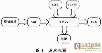
2 FPGA logic function module design The
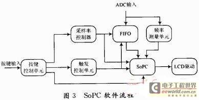
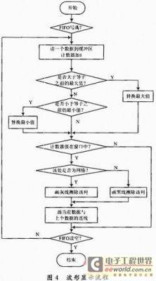
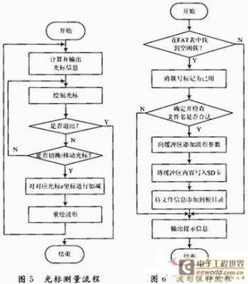
internal system block diagram of FPGA is shown in Figure 2. It is mainly composed of sampling rate controller, trigger control unit, FIFO controller, frequency measurement unit, key control unit and LCD driver. 3 SoPC design The NiosⅡ/f processor is used in this design, using hardware multiplier and divider, working at 50 MHz. The RAM block embedded in FPGA is used as the system's running memory. FLASH is used as an off-chip memory to store user programs, which is connected to the NiosⅡ processor through the Avalon bus tri-state bridge. 3.1 SoPC software design After the system is turned on and calls related functions to initialize LCD, SD card and FAT file system, it first draws the graphical interface and outputs fixed information, then reads the waveform parameters, displays it on the LCD, and then waits for FIFO to be full. If FIFO is full, the FIFO data is read into the buffer, and the waveform is drawn on the screen at the same time to obtain the maximum and minimum values of the waveform. Finally, if there is a user key input, the key event is processed, otherwise the waveform parameters are detected to see if they change, if there is a change, the display is updated, otherwise the FIFO is waited for to be full and the next display is performed. The process is shown in Figure 3. 3.1.1 Design of SoPC bottom-level software The bottom-level software is the driver of each device, mainly including: (1) LCD driver. According to the requirements of display content, the LCD driver designed the following functions: ① Send data/command: send data/command to LCD through the driver; ② LCD initialization: complete LCD power-on reset and initialization; ③ LCD clear screen: clear the display; ④ Output a pixel: output a pixel of a specified color at a specified position; ⑤ Draw a straight line: draw a straight line of a specified color from (x0, y0) to (x1, y1); ⑥ Draw a rectangle: draw a rectangle of a specified color from (x0, y0) to (x1, y1), and you can choose whether to fill it; ⑦ Output a character: output a character of a specified color at a specified position; ⑧ Output a string: output a string of a specified color at a specified position. (2) SD card driver. SD card communication adopts SPI mode, and the functions and features of SD card driver are as follows: ① Send data/command: send data/command to SD card; ② Read data: read one byte from SD card; ③ SD card reset: reset SD card after power-on and make it enter SPI mode; ④ SD card initialization: initialize SD card to prepare for data reading and writing; ⑤ Read a sector: read a sector of data from the specified sector address to the buffer; ⑥ Write a sector: write the buffer data to the specified sector address. (3) FAT16 file system. The main functions and features of FAT16 file system are as follows: ① FAT initialization: obtain FAT information such as the number of sectors per cluster, FAT table address, root directory address and the number of sectors occupied by FAT table; ② Determine file name: search for existing waveform files to determine the name of the file to be saved; ③ Add root directory entry: add the name, size, location, etc. of the saved file to the root directory; ④ Add FAT table entry: search for empty clusters in the FAT table and write the cluster number of the new file into the FAT table. [page] 3.1.2 SoPC top-level software design The top-level software of SoPC mainly completes the functions of waveform and parameter display, run/stop control, cursor measurement, waveform window movement, and data saving to SD card. (1) Waveform parameter display. After drawing the graphical interface, the fixed part of the waveform information is output first, such as Vpp: ???mV, where "???" will be updated after reading the relevant parameters. Then read the relevant parameters and determine whether they have changed. If there is a change, update the relevant display. After the waveform output is completed, update the peak-to-peak value to the screen. (2) Waveform display. After the waveform parameter display is completed, the CPU enters the waiting state. If the FIFO is full, it starts to read the FIFO data and display the waveform. The process is shown in Figure 4. (3) Run/stop control. After the waveform is displayed, if stop is read as 1, it waits until the FIFO is full and enters the stop state. In the stop state, the data in the FIFO remains unchanged. In the stop state, if user input is detected, the corresponding function is executed. If stop is detected as 0, the screen is cleared, the graphical interface is redrawn, the run icon is output, and the waveform display state is returned. (4) Cursor measurement. If the cursor measurement is detected as 1 in the stop state, the cursor measurement state is entered. First, the y-axis coordinates of the two cursors are converted into actual voltage values and output to the LCD. Then, the difference between the two cursor voltages is calculated and output to the corresponding position on the LCD. Then, the x-axis difference between the two cursors is converted into actual time according to the frequency division coefficient and output to the LCD. Finally, two cross cursors are drawn. Each cursor consists of two straight lines, one horizontal and one vertical, and their intersection is located on the waveform. After the cursor is drawn, the user key is detected. If there is a left or right movement or cursor switching key operation, the x-coordinate of the corresponding cursor is added or subtracted. Then, the waveform is re-read from the buffer and output to the LCD, overwriting the previous information. Then, the cursor drawing function is called again to draw the new cursor position and cursor information. The process is shown in Figure 5. (5) Save the waveform to the SD card. If the save key input is detected in the stop state, the data is saved to the SD card. First, search for an empty cluster in the FAT table, return the cluster number, mark the cluster in the FAT table as occupied, and update the FAT table at the same time. Then search for an existing DAT file in the root directory. If there is a DAT file, return the largest file name, otherwise return 0. Then write the data in the buffer to the corresponding sector of the SD card. The sector address = root directory address + root directory size + (cluster number - 2) × number of sectors per cluster. Then find a free item in the root directory and write the file name, size, and cluster to the item to complete the file saving. Finally, output the corresponding prompt information on the LCD. The process is shown in Figure 6. (6) Movement of the waveform display window. If the left/right movement input is detected in the stop state, the waveform display window is moved. When the left/right key is pressed, if the window does not exceed the FIFO boundary, the first address of the window is moved left/right by 2 pixels, and then the displayed window is updated, and the position of the window indicator is updated proportionally. (7) Waveform file format. The file used to save the waveform is named in 8.3 format, named OSC_xxxx. DAT, where xxxx is the file number. Since the amount of waveform data collected each time is the same, the file size is also a fixed value. The FIFO depth is 256 B. After adding information such as trigger level, trigger edge, and time scale, the file size is 260 B. Since the underlying read and write operations of the disk are performed in sectors, and one sector is 512 B, the file size is defined as 512 B. The first 256 B is the waveform data, the 257th B is the trigger edge information, the 258th B is the trigger level information, and the 259th B and 260th B are the frequency division coefficients. The size of the time scale can be obtained after software conversion.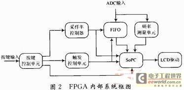
4 PC software design
The PC software is designed in C language. The graphics part uses the SDL library. The PC software is used to open the waveform file saved by the oscilloscope, restore the waveform information, and perform cursor measurement. The program first initializes the SDL video, then opens the file to read 260 bytes, and closes the file. Load the background pattern and initialize the TTF font. Draw the waveform onto the background pattern and calculate the relevant parameters to the corresponding position, draw two cursors, and wait for the user to move the cursor. After the cursor moves, reload the background and waveform and update the relevant information. The software flow is shown in Figure 7. 5 Conclusion This paper introduces a digital oscilloscope design based on SoPC. The actual test results show that the system completes the basic functions of the digital oscilloscope, each part works normally, and each indicator meets the design requirements. In the design process, FPGA chips, embedded NiosⅡ processors and Verilog HDL language are used to simplify the circuit design, improve flexibility and shorten the design cycle.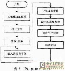
Previous article:Application of Oscilloscope in Switching Power Supply Analysis
Next article:RIGOL digital oscilloscope optimizes the automated measurement solution for lighter production lines
Recommended ReadingLatest update time:2024-11-16 20:26


- Keysight Technologies Helps Samsung Electronics Successfully Validate FiRa® 2.0 Safe Distance Measurement Test Case
- From probes to power supplies, Tektronix is leading the way in comprehensive innovation in power electronics testing
- Seizing the Opportunities in the Chinese Application Market: NI's Challenges and Answers
- Tektronix Launches Breakthrough Power Measurement Tools to Accelerate Innovation as Global Electrification Accelerates
- Not all oscilloscopes are created equal: Why ADCs and low noise floor matter
- Enable TekHSI high-speed interface function to accelerate the remote transmission of waveform data
- How to measure the quality of soft start thyristor
- How to use a multimeter to judge whether a soft starter is good or bad
- What are the advantages and disadvantages of non-contact temperature sensors?
- Innolux's intelligent steer-by-wire solution makes cars smarter and safer
- 8051 MCU - Parity Check
- How to efficiently balance the sensitivity of tactile sensing interfaces
- What should I do if the servo motor shakes? What causes the servo motor to shake quickly?
- 【Brushless Motor】Analysis of three-phase BLDC motor and sharing of two popular development boards
- Midea Industrial Technology's subsidiaries Clou Electronics and Hekang New Energy jointly appeared at the Munich Battery Energy Storage Exhibition and Solar Energy Exhibition
- Guoxin Sichen | Application of ferroelectric memory PB85RS2MC in power battery management, with a capacity of 2M
- Analysis of common faults of frequency converter
- In a head-on competition with Qualcomm, what kind of cockpit products has Intel come up with?
- Dalian Rongke's all-vanadium liquid flow battery energy storage equipment industrialization project has entered the sprint stage before production
- Allegro MicroSystems Introduces Advanced Magnetic and Inductive Position Sensing Solutions at Electronica 2024
- Car key in the left hand, liveness detection radar in the right hand, UWB is imperative for cars!
- After a decade of rapid development, domestic CIS has entered the market
- Aegis Dagger Battery + Thor EM-i Super Hybrid, Geely New Energy has thrown out two "king bombs"
- A brief discussion on functional safety - fault, error, and failure
- In the smart car 2.0 cycle, these core industry chains are facing major opportunities!
- The United States and Japan are developing new batteries. CATL faces challenges? How should China's new energy battery industry respond?
- Murata launches high-precision 6-axis inertial sensor for automobiles
- Ford patents pre-charge alarm to help save costs and respond to emergencies
- New real-time microcontroller system from Texas Instruments enables smarter processing in automotive and industrial applications
- [Welcome to the New Year and National Day] DCExpert takes you to "full stack" hands-on: rechargeable touch-controlled creative LED lamp based on ESP8266
- Mir MYC-YT507 development board review: Play NES games with the Famicom
- [RT-Thread reading notes] Week 4: Digest the first six chapters and fill in the gaps
- Steam oven water level detection - which one is more suitable, the float type or the photoelectric type?
- POE PD+DCDC non-isolated solution
- Help: Transformer detection of low frequency or DC residual current
- How to realize network remote control of balance car? ?
- Help with max30102 heart rate and blood oxygen test module issues
- Espressif releases new products really fast: the first Wi-Fi 6 + Bluetooth 5 (LE) RISC-V SoC is released
- Have you ever encountered these problems: 5 times the salary cannot retain employees?

 Principles and Applications of Wireless Sensor Networks (Tang Hong)


 京公网安备 11010802033920号