1. Introduction
An image sensor is a functional device that uses the light-to-electric conversion function of a photoelectric device to convert the light image on its photosensitive surface into an electrical signal "image" that is proportional to the light image.
A solid-state image sensor refers to an integrated, functionalized photoelectric device consisting of a number of photosensitive units and a shift register arranged on the same semiconductor substrate. Photosensitive units are referred to as "
pixels
" or "pixels", which are spatially and electrically independent of each other. A solid-state image sensor uses the photoelectric conversion function of a photosensitive unit to
convert the
optical
image projected onto the photosensitive unit into an electrical signal "image", that is, to convert the spatial distribution of light intensity into a spatial distribution of charge packets of varying sizes that are proportional to the light intensity. Then, the function of the shift register is used to read and output these charge packets under the control of clock pulses, forming a series of timing pulse sequences of varying amplitudes.
Compared with ordinary image sensors, solid-state image sensors have the characteristics of small size, low distortion, high sensitivity, vibration resistance, moisture resistance and low cost. These characteristics determine that it can be widely used in automatic control and automatic measurement, especially in image recognition technology. This article starts with analyzing the principles of solid-state image sensors and focuses on analyzing and discussing them in the fields of measurement and control and image recognition.
2. Charge Coupled Devices and Working Principles
Charge Coupled Devices (
CCDs
) are sensitive devices of solid-state image sensors. Like ordinary MOS, TTL and other circuits, they are integrated circuits, but CCDs have many unique functions such as photoelectric conversion, signal storage, transfer (transmission), output, processing and electronic shutter.
The basic principle of charge coupled devices (CCDs) is to apply appropriate pulse voltages to a series of MOS capacitor metal electrodes to repel the majority carriers in the semiconductor substrate, forming a "potential well" movement, and then achieve the transfer of signal charges (minority carriers). If the transferred signal charge is generated by light image irradiation, the CCD has the function of an image sensor; if the transferred charge is obtained by external injection, the CCD can also have functions such as delay, signal processing, data storage and logical operations. The
basic principle of charge coupled devices (CCDs) is closely related to the physical mechanism of metal oxide silicon (MOS) capacitors. Therefore. First, analyze the principle of MOS capacitors.
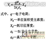
Figure 1 shows a MOS capacitor formed by depositing metal on a thermally oxidized P-type Si (p-Si) substrate. If a forward voltage is applied to its metal electrode at a certain moment, the majority carriers in the p-Si (holes at this time) will be repelled, so a depletion region will be formed on the Si surface. This depletion region is the same as the ordinary pn junction, and is also a space charge region composed of ionized acceptors. Moreover, under certain conditions, the larger the , the deeper the depletion layer. At this time, the potential (i.e., surface potential V) of the Si surface to absorb minority carriers (electrons at this time) is also greater. Obviously, the amount of minority carrier charge that the MOS capacitor can accommodate at this time is greater. Based on this, the image metaphor of "surface potential well" (abbreviated as potential well) can be used to illustrate the ability of MOS capacitors to store (signal) charges under the action of V (or in V). Conventionally, the potential well is imagined as a bucket, and the minority carriers (signal charges) are imagined as the fluid at the bottom of the bucket. When analyzing solid-state devices, the potential inside the semiconductor substrate is often taken as zero, so it is more convenient to take the positive value of the surface potential ring with the increasing direction pointing downward (Figure 1(b)).

Figure 3 MOS capacitor and its surface potential well concept
The surface potential V is a very important physical quantity. In the case shown in Figure 1Ca), if the added Vc does not exceed a certain limit value, the surface potential is:

The above formula is obtained by solving the Poisson equation for the potential distribution in the semiconductor. Since Xa is controlled by VG, V is also a function of Vc.
There are two ways to generate the charge (minority carriers) of a CCD: voltage signal injection and light signal injection. As an image sensor, CCD receives light signals, that is, light signal injection method. When the light signal is irradiated onto the CCD silicon chip, the depletion region near the gate absorbs photons to generate electron-hole pairs. At this time, under the action of the gate voltage, the majority carriers (holes) will flow into the substrate, while the minority carriers (electrons) will be collected in the potential well to form signal charges and store them.
In this way, those photons that are higher than the semiconductor bandgap width can establish a storage charge proportional to the light intensity.
The CCD composed of many MOS capacitors generates signal charges of photogenerated carriers under the irradiation of light images, and then enables it to have the self-scanning function of transferring signal charges, that is, to form a solid-state image sensor.
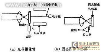
Figure 2 is a comparison of the basic principles of a photoconductive camera tube and a solid-state image sensor. In Figure 2ta), when the incident light image signal is irradiated onto the surface of the middle electrode of the camera tube, a potential distribution proportional to the amount of light irradiated at each point will be generated on it. If the middle electrode is scanned by an electron beam, a variable discharge current will be generated on the load Rl. The load current changes due to the different light amounts, which is exactly the desired output electrical signal. The deflection or focusing of the electron beam is achieved by magnetic or electric field control.
 ~[.bD W ;
Figure 2 Comparison of the basic principles of a photoconductive camera tube and a solid-state image sensor
The output signal of the solid-state image sensor shown in Figure 2(b) does not require an external scanning electron beam, and can be directly obtained by self-scanning the pixels on the semiconductor substrate. Such an output electrical signal corresponds to the position of its corresponding pixel, which is undoubtedly more accurate, and the distortion of the regenerated image is extremely small. Obviously, it is often difficult to avoid the distortion of the regenerated image caused by the deflection distortion or focus change of the scanning electron beam or other reasons for image sensors such as photoconductive camera tubes.
Solid-state image sensors with extremely low distortion are very suitable for testing technology and image recognition technology. In addition, compared with camera tubes, solid-state image sensors have many advantages such as small size,
light
weight
, durability, impact resistance, vibration resistance, strong anti-electromagnetic interference ability, and low power consumption, and the cost of solid-state image sensors is also low.
3. Classification, structure and characteristics of solid-state sensors
From the perspective of use, solid-state image sensors can be divided into two categories: linear and area solid-state image sensors. According to the different sensitive devices used, they can be divided into CCD, MOS linear sensors and CCD, MOS area sensors. Linear solid-state image sensors are mainly used in testing, fax and optical character recognition technology, while the development direction of area solid-state image sensors is mainly used as small cameras for tape recording. This article mainly introduces the structure of linear solid-state image sensors commonly used in engineering testing.
Figure 3 shows the structure of a linear solid-state image sensor. Its photosensitive part is a linear array of photosensitive diodes. 1728 PDs are located in the center of the sensor as photosensitive pixels, and CCD conversion registers are set on both sides. The register is covered with a light shield. The signal charge of the odd-numbered PD is transferred to the transfer register on the lower side; the even-numbered PD is transferred to the transfer register on the upper side. The CCD transfer register is driven by another signal, and the signal charge is read out from the photosensitive diode PD in sequence through the common output terminal.
 4y.] x 6
Figure 3 Structure of a linear solid-state image sensor

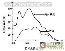
Usually, the photosensitive diode of the photosensitive part is made into MOS form, and the electrode is made of polysilicon. Although the polysilicon film can transmit light images. However, it has a strong absorption effect on blue light. Especially when fluorescent lamps are used as light sources, the blue light spectrum response of the sensor will become extremely poor. In order to improve this situation, a light window can be opened on the polysilicon electrode. Since the photogenerated signal charge of the sensor of this structure is generated and accumulated in the MOS capacitor, the capacity is increased and the dynamic range is greatly expanded. Figure 5 is its spectral response characteristics. The dotted line in the figure represents the sensor characteristics of the CCD using only polysilicon electrodes without opening a light window; the solid line represents the PD formed by opening a light window, and the CCD sensor characteristics of the signal charge accumulated in the MOS container. Obviously, the blue spectrum response characteristics of the latter are significantly improved and improved, so the latter is called a high-sensitivity linear solid-state image sensor.

Figure 5 High sensitivity sensor
The main characteristics of solid-state image sensors are:
①. Modulation transfer function
MTF
characteristics: Solid-state image sensors are composed of pixel matrices and corresponding transfer parts. Although solid-state pixels have been made very small and their intervals are also very small, this is still the main obstacle to identifying tiny images or reproducing subtle parts of images.
②. Output saturation characteristics: When a strong light image above the saturation exposure is irradiated onto the image sensor, the output voltage of the sensor will be saturated. This phenomenon is called output saturation characteristics. The fundamental reason for the output saturation phenomenon is that photodiodes or MOS capacitors can only generate and accumulate photogenerated signal charges within a certain limit.
③. Dark output characteristics: Dark output is also called no-light output, which refers to the characteristic that the sensor still has a tiny output when there is no light image signal irradiated. The output comes from the dark (no-light) current. ④
. Sensitivity: The output photocurrent generated by unit radiation illumination represents the sensitivity of the solid-state image sensor, which is mainly related to the pixel size of the solid-state image sensor.
⑥. Scattering: Over-bright light images above the saturation exposure will generate and accumulate over-saturated signal charges in the pixels. At this time, the over-saturated charges will diffuse from the potential well of one pixel through the substrate to the potential well of the adjacent pixel. In this way, places on the regenerated image that should not show a certain brightness will show brightness instead. This situation is called the diffusion phenomenon.
⑥. Afterimage: After scanning a pixel and reading out its signal charge, the phenomenon that the readout signal after the next scan is still affected by the remaining signal charge from the last time is called afterimage.
;*
Previous article:CCD Sensor and Its Application
Next article:Image Sensor
Recommended ReadingLatest update time:2024-11-16 19:34


- Melexis launches ultra-low power automotive contactless micro-power switch chip
- Infineon's PASCO2V15 XENSIV PAS CO2 5V Sensor Now Available at Mouser for Accurate CO2 Level Measurement
- Milestone! SmartSens CMOS image sensor chip shipments exceed 100 million units in a single month!
- Taishi Micro released the ultra-high integration automotive touch chip TCAE10
- The first of its kind in the world: a high-spectral real-time imaging device with 100 channels and 1 million pixels independently developed by Chinese scientists
- Melexis Launches Breakthrough Arcminaxis™ Position Sensing Technology and Products for Robotic Joints
- ams and OSRAM held a roundtable forum at the China Development Center: Close to local customer needs, leading the new direction of the intelligent era
- Optimizing Vision System Power Consumption Using Wake-on-Motion
- Infineon Technologies Expands Leading REAL3™ Time-of-Flight Portfolio with New Automotive-Qualified Laser Driver IC
- Innolux's intelligent steer-by-wire solution makes cars smarter and safer
- 8051 MCU - Parity Check
- How to efficiently balance the sensitivity of tactile sensing interfaces
- What should I do if the servo motor shakes? What causes the servo motor to shake quickly?
- 【Brushless Motor】Analysis of three-phase BLDC motor and sharing of two popular development boards
- Midea Industrial Technology's subsidiaries Clou Electronics and Hekang New Energy jointly appeared at the Munich Battery Energy Storage Exhibition and Solar Energy Exhibition
- Guoxin Sichen | Application of ferroelectric memory PB85RS2MC in power battery management, with a capacity of 2M
- Analysis of common faults of frequency converter
- In a head-on competition with Qualcomm, what kind of cockpit products has Intel come up with?
- Dalian Rongke's all-vanadium liquid flow battery energy storage equipment industrialization project has entered the sprint stage before production
- Allegro MicroSystems Introduces Advanced Magnetic and Inductive Position Sensing Solutions at Electronica 2024
- Car key in the left hand, liveness detection radar in the right hand, UWB is imperative for cars!
- After a decade of rapid development, domestic CIS has entered the market
- Aegis Dagger Battery + Thor EM-i Super Hybrid, Geely New Energy has thrown out two "king bombs"
- A brief discussion on functional safety - fault, error, and failure
- In the smart car 2.0 cycle, these core industry chains are facing major opportunities!
- The United States and Japan are developing new batteries. CATL faces challenges? How should China's new energy battery industry respond?
- Murata launches high-precision 6-axis inertial sensor for automobiles
- Ford patents pre-charge alarm to help save costs and respond to emergencies
- New real-time microcontroller system from Texas Instruments enables smarter processing in automotive and industrial applications
- What are the differences between DK251 CA251 A251 on KEIL website, with pictures
- RT-Thread4.0 is officially released, and also supports SMP (source code download address included)
- Help! 50Mhz sine signal output problem?
- Smart speakers are more than just listening - TI DLP Pico technology creates an excellent smart display experience
- What about emoticons?
- Design tips video generated by machine learning algorithm
- [Qinheng RISC-V core CH582] Use Bluetooth Peripheral routines to experience Bluetooth sending and receiving data functions for the first time
- EEWORLD University Hall----Live Replay: Application of NXP LPC553x in Dual Motor Control
- 【TI Course】How can I learn the complete course? How do I need to pay and how do I pay?
- E-sports support

 Image acquisition and processing system for panoramic map applications
 光电探测技术与系统 (付小宁 牛建军 陈靖 (编著))


 京公网安备 11010802033920号