|
introduction With the continuous improvement of people's requirements for real-time signal processing and the rapid development of large-scale integrated circuits, digital signal processor DSP chips, which are the core and symbol of digital signal processing, have been rapidly developed and applied. It can be widely used in real-time signal processing fields such as communication systems, graphics/image processing, radar sonar, and medical signal processing. As far as ADI is concerned, following the 16-bit fixed-point ADSP21xx and 32-bit floating point ADSP21xxx series, it has recently launched a new device in the TigerSHARC series. This article introduces the design of an image acquisition and processing system using the ADSP-TS201S chip in this series. The system can complete image collection, processing and display, thereby realizing intelligent signal processing for target recognition and tracking. This system collects digital and analog video data from the camera, and displays it on the PC through the PCI bus after processing. The entire system mainly consists of three parts: video signal acquisition module, DSP image processing module, and PCI interface module (Figure 1).
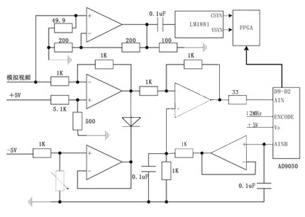
·Video signal acquisition module The camera provides two video signals: one analog video and one digital video. After the analog video signal is clamped, corrected and amplified, the signal is sent to the A/D converter, and then the video signal is latched by the FPGA and sent to DSP1; through the video synchronization separation circuit, the LM1881 separates the analog video lines and Field synchronization signal is used to control the acquisition of video data to DSP1 for image processing. The clamp correction and video synchronization circuit is shown in Figure 2. The analog video is input through the op amp, and the center level is adjusted to 3.3V and added to the A/D input. The A/D converted data enters the FPGA latch. The op amps all use ADI's AD8047AR, and the A/D converters use ADI's AD9050. AD9050 is a 10-bit A/D converter, and the upper 8 bits are entered into the FPGA. The sampling clock is 12MHz, which is the same as the digital video signal. It is generated by FPGA dividing the 48MHz clock by four.
The digital video signal of the camera is 14 pairs of differential signals. The differential signals are converted into single-ended signals by the FPGA and the data is latched. 14 bits per pixel, 320×240 per frame. The FPGA uses ALTERA's CYCLONE series EP1C3T144C-6, and the configuration chip uses EPC2LC20. EP1C3T144C-6 has a dedicated I/O port for converting differential signals to single-ended signals. The digital and analog video signals latched in the FPGA are output to the DSP1 data bus according to the working mode selection, and are read and processed by DSP1. The data rate is the same as the sampling rate of analog video and the data rate of digital video. Working mode selection and switch control are introduced to FPGA through PIC9054. ·DSP processor module The DSP processor array module mainly consists of four high-speed and high-performance DSP processing chips ADSP-TS201S to form a multi-DSP processor system. The performance of ADSP-TS201S is as follows: The basic performance indicators are as follows: DSP1 in the DSP processor array module is used to sort out the collected video signals, perform corresponding preprocessing, and then distribute the data to the subsequent DSP for further processing. The DSP1 parallel port should be connected to the video data output by the FPGA, and also connected to FLASH to complete DSP loading. IRQ0 and IRQ1 of DSP1 are used as frame interrupt and line interrupt of video input respectively, and are connected to FPGA. The connection circuit is shown in Figure 3 below. FLASH uses AMD's AM29LV017D, which is a 2M x 8-Bit memory. FLASH can be programmed through DSP1. It is necessary to ensure that when reading and writing FLASH, the data output bus D0~D13 of FPGA is high impedance. On the contrary, when the data channel is running, , the FLASH output should also be made high impedance, so use BMS to select FLASH.
DSP2 and DSP3 in the DSP processor array module are used to implement the main algorithms in image processing. DSP2 and DSP3 use link ports to connect to DSP1 respectively to receive the data transmitted from DSP1. DSP2 and DSP3 also use link ports to connect to DSP4 respectively, and transmit the processed data to DSP4 through the link port for the next step of processing and data processing. tidy. In addition, DSP2 and DSP3 are also directly connected using link ports to realize the channel between DSP2 and DSP3, so that DSP2 and DSP3 can be easily configured into pipeline or parallel processing modes. DSP4 in the DSP processor array module receives the data sent by DSP2 and DSP3. After further processing, the final processed data is sent to the dual-port RAM through the data bus, and the data is sent to the PC through the PCI interface chip PCI9054. This dual-port RAM uses three pieces of IDT70LV27 (32K x 16-Bit) to form a 96K After a frame of image data is filled, an interrupt is generated to the PC and the PC is requested to read the data. When the PC finishes reading a frame of image data, it should provide a corresponding response to allow DSP4 to refresh the dual-port RAM. The DSP array machine interconnection circuit is shown in Figure 1, and the connection between DSP4 and dual-port RAM is shown in Figure 4. DSP4 is connected to three pieces of dual-port RAM to form an interface with PCI9054. FLAG0 of DSP4 serves as the video transmission handshake signal output through PCI9054. The ADSP-TS201S array machine adopts the link port interconnection method, and sets the data transmission start FLAG signal in the main data transmission direction to generate an interrupt on the receiver's IRQ to better achieve timing matching. DSP1 introduces the work/off selection (FLAG1 input), and the data mode (digital/analog) selection is read in by the DATA14 pin. When a frame of data starts to be input, the data selection mode can be read once, and then it can no longer be processed. .
| ||||
| ·PCI interface module
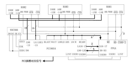
The PCI interface adopts PLX's PCI9054 interface chip, 32-bit, 33MHZ data bus. Three pieces of dual-port RAM (IDT70LV27) RAM1, 2, and 3 are used as DSP4 data output buffer. Read into PC by PCI9054. In the dual-port RAM, it is equivalent to the right half of the interface. The circuit connection of PCI9054 is shown in Figure 5. PCI9054 corresponds to the signal of the PCI slot, connect according to the PCI slot name, and select 93CS66 to load the EEPROM. Introducing LD0~LD3 into the FPGA can output 4-bit status in a single I/O write mode for host control. On and off, digital video/analog video selection uses one of the decoders of A16~17 as the address selection. After FPGA reads it in, it decodes it into a control signal and outputs it.
The image acquisition and processing system based on ADSP-TS201S can complete high-speed image processing, realize real-time display of images, and target tracking. In practical applications, the system works stably and achieves the expected results. |
Previous article:Extend TINI’s IO performance
Next article:Hardware design of digital signal processor based on PCI bus
Recommended ReadingLatest update time:2024-11-16 16:44


- Popular Resources
- Popular amplifiers
-
 Point Cloud Registration from Beginner to Master (Guo Hao)
 -
 A review of learning-based camera and lidar simulation methods for autonomous driving systems
 -
 Semantic Segmentation for Autonomous Driving: Model Evaluation, Dataset Generation, Viewpoint Comparison, and Real-time Performance
 -
 Digilent Vivado library
- Huawei's Strategic Department Director Gai Gang: The cumulative installed base of open source Euler operating system exceeds 10 million sets
- Analysis of the application of several common contact parts in high-voltage connectors of new energy vehicles
- Wiring harness durability test and contact voltage drop test method
- Sn-doped CuO nanostructure-based ethanol gas sensor for real-time drunk driving detection in vehicles
- Design considerations for automotive battery wiring harness
- Do you know all the various motors commonly used in automotive electronics?
- What are the functions of the Internet of Vehicles? What are the uses and benefits of the Internet of Vehicles?
- Power Inverter - A critical safety system for electric vehicles
- Analysis of the information security mechanism of AUTOSAR, the automotive embedded software framework
 Professor at Beihang University, dedicated to promoting microcontrollers and embedded systems for over 20 years.
- Innolux's intelligent steer-by-wire solution makes cars smarter and safer
- 8051 MCU - Parity Check
- How to efficiently balance the sensitivity of tactile sensing interfaces
- What should I do if the servo motor shakes? What causes the servo motor to shake quickly?
- 【Brushless Motor】Analysis of three-phase BLDC motor and sharing of two popular development boards
- Midea Industrial Technology's subsidiaries Clou Electronics and Hekang New Energy jointly appeared at the Munich Battery Energy Storage Exhibition and Solar Energy Exhibition
- Guoxin Sichen | Application of ferroelectric memory PB85RS2MC in power battery management, with a capacity of 2M
- Analysis of common faults of frequency converter
- In a head-on competition with Qualcomm, what kind of cockpit products has Intel come up with?
- Dalian Rongke's all-vanadium liquid flow battery energy storage equipment industrialization project has entered the sprint stage before production
- Allegro MicroSystems Introduces Advanced Magnetic and Inductive Position Sensing Solutions at Electronica 2024
- Car key in the left hand, liveness detection radar in the right hand, UWB is imperative for cars!
- After a decade of rapid development, domestic CIS has entered the market
- Aegis Dagger Battery + Thor EM-i Super Hybrid, Geely New Energy has thrown out two "king bombs"
- A brief discussion on functional safety - fault, error, and failure
- In the smart car 2.0 cycle, these core industry chains are facing major opportunities!
- The United States and Japan are developing new batteries. CATL faces challenges? How should China's new energy battery industry respond?
- Murata launches high-precision 6-axis inertial sensor for automobiles
- Ford patents pre-charge alarm to help save costs and respond to emergencies
- New real-time microcontroller system from Texas Instruments enables smarter processing in automotive and industrial applications
- Physical Design Analysis of PCB Board in Switching Power Supply Design
- PCB Design
- Why can't I see the bluetooth function when running micropython on EPS32?
- Does anyone know how this kind of colored PCB is made? ?
- EEWORLD University Hall----Live Replay: Comprehensive explanation of TI MSP Academy tutorial
- TI CC2640R2F documentation for beginners
- [MM32 eMiniBoard Review] In-depth understanding of HID-2
- New version of WEBENCH user guide
- [FS-IR02 + D1CS-D54] - 5: Linking with MCU (D1CS-D54)
- Qorvo Acquires UWB Software Provider 7Hugs Labs SAS


 Point Cloud Registration from Beginner to Master (Guo Hao)
 Digilent Vivado library


 京公网安备 11010802033920号