1 USB control chip
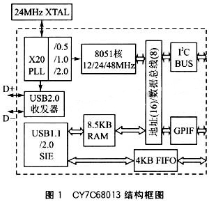
Cypress's EZ-USB FX2 series of chips is one of the earliest microcontrollers compliant with the USB2.0 protocol. It integrates a transceiver (transceiver), serial interface engine (SIE), enhanced 8051 core and programmable peripheral interface (GPIF). The unique structure of the FX2 series chips enables the data transmission speed to reach up to 56Mbps, maximizing the Meets the bandwidth of USB2.0.
The structural block diagram of CY7C68013 is shown in Figure 1.
 |
|---|
The endpoint buffer of FX2 is divided into two groups: EP0, EP1 (IN), and EP1 (OUT) are small endpoints with a size of 64 bytes. They can only be accessed by the CPU and cannot be connected by external logic; EP2, EP4, and EP6 , EP8 is a large configurable endpoint, EP2 and EP4 default to OUT endpoints, EP6 and EP8 default to IN endpoints. FX2 provides a variety of buffering methods for its large endpoints to meet the requirements for high bandwidth in transmission. During the transmission process, EZ-USB FX2 reads the data uploaded to the host from the IN buffer and writes it in the OUT buffer for the external processor. read data. It has two transmission rates: full speed (12Mbps) and high speed (480Mbps), and has 4 transmission modes specified by the USB protocol, namely control transmission (control mode), interrupt transmission (interrupt mode), block transmission (bulk mode) and Isochronous mode.
2 System hardware architecture
2.1 Hardware connection between USB and DSP
The digital signal processor selected in the system is the TMS320C6713 in the C6000 floating point series released by TI. Its peak processing speed can reach 1350MFLOPS (million floating point operations/s). Peripheral resources include direct memory access controller (DMA), external memory interface (EMIF), serial port, expansion bus or host port, timer, etc. In the system, its EMIF port is used to connect the programmable logic chip CPLD to expand the USB control interface. CY7C68013 can realize the interface with DSP or MCU very flexibly. When it is used as a master device, the general programmable interface (GPIF) has programmable waveform descriptors and configuration registers and can be easily compatible with most bus standards. When it is used as a slave device, a 4KB large-capacity FIFO is used for data Buffering simplifies the external hardware design of the interface and can be connected to the main device (such as ASIC, DSP, etc.) in a synchronous or asynchronous manner.
In this solution, it is used as a slave device and uses Slave FIFOs to read/write asynchronously. In this mode, the DSP can read/write the multi-layer buffer FIFO inside the CY7C68013 just like reading/writing a normal FIFO. The main signal connections are shown in Figure 2. When the host (PC) issues a command, PA3 also provides an interrupt trigger signal to the external interrupt pin 6 (EXT_INT6) of the DSP. After its rising edge is detected, the DSP enters the corresponding interrupt service program and starts processing the USB transmission. The DSP reads, writes and enables the CY7C68013 through CPLD. The "OR" combination logic meets strict timing requirements. FLAGB and FLAGC are CY7C68013 internal FIFO empty and full status flags, PA[0:1] indicates the command type sent by the PC. This information is integrated into the data bus ED[0:15] inside the CPLD. The DSP extracts and judges the data packet before starting to transmit it. TMS320C6713 selects the internal endpoint (EP) of CY7C68013 through the address line TEA[2:3]. .
 |
|---|
2.2 Overall structure design of the system
Based on the above hardware communication mode, a master-slave system based on PC, USB, and DSP is built. When the system is powered on and completes the firmware configuration and hardware initialization of each module, the PC can issue control commands and use external signals to trigger the DSP to enter the corresponding interrupt processing program. Automatically complete the multiple cycle processes of data stream USB download, DSB processing and USB return; the PC displays the processed results. The overall structure block diagram of the system is shown in Figure 3.
 |
|---|
The DSP chip provides interfaces for SDRAM, Flash and other devices through the EMIF in the chip (including 4 storage spaces CE[0:3]). SDRAM is a synchronous memory device, and EMIF has dedicated control lines and clocks to seamlessly connect it (CE0 space). Here SDRAM is used as data memory.
For the C6000 series DSP, the debugged application needs to be solidified so that it can be automatically loaded and run when the system is powered on. The solution uses Flash startup boot mode, which is located in the EMIF asynchronous interface CE1 space.
The reset circuit provides automatic reset and manual control reset when the system is powered on and the working voltage is abnormal. The clock circuit provides clock signals to the DSP processing module.
The USB interface circuit provides a high-speed data transmission channel between PC and DSP. The interface chip is connected to the external processor DSP through CPLD and placed in the CE2 space of EMIF (the communication mode is as mentioned above).
3 Communication module software design
In order to simplify and accelerate the development process of USB peripherals for users using the EZ-USB FX2 chip, Cypress has specially designed the CY7C68013 development board and comes with a development kit that contains a driver and application program necessary for USB peripherals. As well as a complete firmware program framework, this framework can perform the initialization of the EZ-USB chip, the processing of USB standard device requests and USB suspend power management services; the user only needs to provide a USB descriptor table and add other endpoints to receive and send The communication code for data and the program code for controlling peripheral circuits are enough.
3.1 Firmware program planning of CY7C68013
The firmware program framework implements a simple interoperable task executor through several different functional modules. First, all internal state variables are initialized by calling the user's initialization function TD_Init(). After that, the program framework initializes the USB port to Configure the status, and enable interrupts, and start to re-enumerate the device at 1s intervals until endpoint 0 receives the setting packet. Once it is detected that endpoint 0 receives more than one setting packet, the firmware framework program starts to execute an interoperable The task allocator repeatedly performs the following tasks in the given order: calls the function TD_Poll(), determines whether there are standard device requests waiting to be processed, and determines whether the USB core reports a USB suspend event.
The main firmware configuration is as follows:
1) Configure the Asynchronous Slave FIFO (Asynchronous Slave FIFO) mode, and the interface driver uses the internal 48MHz clock source.
2) EndPoint4 and EndPoint8 serve as bidirectional transmission pipes and correspond to buffer FIFO4 and FIFO8 respectively to store the data that USB needs to receive and download. They all adopt the batch (BULK) transmission method, which is more reliable than other transmission methods defined by USB2.0. , high transmission rate and other characteristics, it is the most commonly used transmission method.
3) Set FIFO4 and FIFO8 to automatic mode, that is, there is no need for the 8051 core of CY7C68013 to participate in the data transmission process to ensure continuous, high-speed, and effective data transmission.
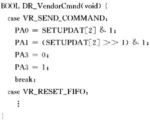
The EZ-USB FX2 chip defines several special registers to assist the firmware program in responding to device requests and transmitting data to the host. When the device receives the setup package, the USB core will automatically put the setup data into the 8-byte SETUPBUF buffer. , users only need to read the setting data from it and analyze it to determine the type of request.
Some of the device request codes in the solution are as follows:
 |
|---|
The second byte in the read buffer is sent to the DSP by PA[0:1] as a command type flag (00 is download, 01 is upload, 10 is processing); at the same time, PA3 port provides the rising edge of the external interrupt trigger signal .
After the firmware is ready, it is loaded into the EEPROM through the Control Panel tool provided by Cypress. When the firmware needs to be modified, the modified firmware on the host can be re-downloaded without changing the hardware.
3.2 Host computer process
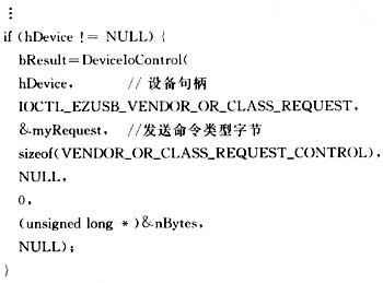
The host application interacts with the operating system, using the rich resources of the PC to implement display verification and improve the operability of the system. When the operating system thinks that a new device is connected, it will automatically call the corresponding device driver. In addition, the software requires a graphical user interface to control the functions used. Here, VC++6.0 is used to compile the application program. First, CreateFile() is called to open the USB interface device and obtain the device handle hDevice. Then the computer calls the DeviceIoControl() function to issued by the peripheral. Part of the procedure is as follows:
 |
|---|
The eight member variables of myRequest correspond to the 8-byte (SETUPDAT) data in the firmware configuration SETUPBUF buffer. The value of value represents the command type (00/01/10) sent by the host to the DSP, so that the DSP can cooperate to complete the reception and processing. and upload system process.
 |
|---|
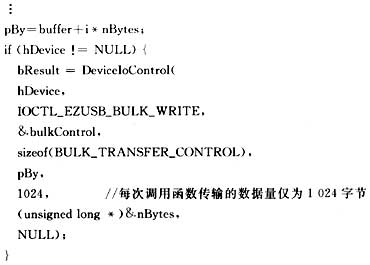
The amount of data transferred each time the DeviceIoControl function is called is only 1KB. In order to meet the requirements of large data volume or whole frame image data transmission, the DeviceIoControl() function needs to be called in a loop. Taking the process of downloading the data stream as an example, the code in the loop body is as follows:
 |
|---|
buffer is the head pointer of the data block sent by the host; pBy is the first address of the data block each time it is downloaded, which is the value that increases with the loop variable i. Similarly, there are similar storage operations during the process of uploading data.
4 system test
This master-slave online system is tested using image sequences.
Trigger the interface control on the PC (PA (0:1) = 00), download 10 images of the same content contaminated by noise from different programs, and the DSP detects the signal of the general external interrupt port EXT_INT6 (corresponding to PA3 of the USB chip) and reads it in Data read command type, store 10 frames of image data into the SDRAM space. After that, the host computer continues to issue processing commands. The DSP detects that PA[0:1]=10 and accumulates and averages the stored multi-frame image data, thereby improving the image quality. When receiving the upload command (PA[0:1]=01), the DSP will send the processed image back to the PC for display.
Conclusion:
This article introduces in detail the hardware connection through the EMIF extended USB interface of TMS32C6713, the development of USB2.0 firmware programs and applications, and the construction of a small online system based on this communication mode. After actual verification, the system operates reliably and is a relatively good solution for high-speed data transmission and processing.
Previous article:DSP implementation of FIR digital filters of different orders
Next article:Interface design of high-speed data acquisition system based on FPGA
Recommended ReadingLatest update time:2024-11-17 02:50


- Popular Resources
- Popular amplifiers
- Huawei's Strategic Department Director Gai Gang: The cumulative installed base of open source Euler operating system exceeds 10 million sets
- Analysis of the application of several common contact parts in high-voltage connectors of new energy vehicles
- Wiring harness durability test and contact voltage drop test method
- Sn-doped CuO nanostructure-based ethanol gas sensor for real-time drunk driving detection in vehicles
- Design considerations for automotive battery wiring harness
- Do you know all the various motors commonly used in automotive electronics?
- What are the functions of the Internet of Vehicles? What are the uses and benefits of the Internet of Vehicles?
- Power Inverter - A critical safety system for electric vehicles
- Analysis of the information security mechanism of AUTOSAR, the automotive embedded software framework
 Professor at Beihang University, dedicated to promoting microcontrollers and embedded systems for over 20 years.
- Innolux's intelligent steer-by-wire solution makes cars smarter and safer
- 8051 MCU - Parity Check
- How to efficiently balance the sensitivity of tactile sensing interfaces
- What should I do if the servo motor shakes? What causes the servo motor to shake quickly?
- 【Brushless Motor】Analysis of three-phase BLDC motor and sharing of two popular development boards
- Midea Industrial Technology's subsidiaries Clou Electronics and Hekang New Energy jointly appeared at the Munich Battery Energy Storage Exhibition and Solar Energy Exhibition
- Guoxin Sichen | Application of ferroelectric memory PB85RS2MC in power battery management, with a capacity of 2M
- Analysis of common faults of frequency converter
- In a head-on competition with Qualcomm, what kind of cockpit products has Intel come up with?
- Dalian Rongke's all-vanadium liquid flow battery energy storage equipment industrialization project has entered the sprint stage before production
- Allegro MicroSystems Introduces Advanced Magnetic and Inductive Position Sensing Solutions at Electronica 2024
- Car key in the left hand, liveness detection radar in the right hand, UWB is imperative for cars!
- After a decade of rapid development, domestic CIS has entered the market
- Aegis Dagger Battery + Thor EM-i Super Hybrid, Geely New Energy has thrown out two "king bombs"
- A brief discussion on functional safety - fault, error, and failure
- In the smart car 2.0 cycle, these core industry chains are facing major opportunities!
- Rambus Launches Industry's First HBM 4 Controller IP: What Are the Technical Details Behind It?
- The United States and Japan are developing new batteries. CATL faces challenges? How should China's new energy battery industry respond?
- Murata launches high-precision 6-axis inertial sensor for automobiles
- Ford patents pre-charge alarm to help save costs and respond to emergencies
- The waveform of the zero line at the input end of the three-phase uncontrolled rectifier to the negative pole of the output voltage
- I have a small question for everyone.
- Smart water meter
- 【NXP Rapid IoT Review】W5 Final Summary
- Why don't the numbers match? I've refreshed it several times, but they still don't match. How come the administrator didn't notice it all these years?
- Comparison between fixed-point dsp and floating-point dsp
- Reliability Design of PCB Board for High-speed DSP System
- How to daisy chain 485
- Silergy SY5072 specification sheet help
- Please help me find out which movie the characters in the attached picture are from. Thank you.

 MATLAB and FPGA implementation of wireless communication


 京公网安备 11010802033920号