Introduction
RS error correction code is one of the most effective and widely used error control codes. It is a multi-base BCH code with strong error correction capability and a typical algebraic geometry code. It was first constructed by Reed and Solomon in 1960 using MS polynomials.
RS codes are widely used in error control systems to improve data reliability, and can be used to construct other code classes, such as cascade codes. RS codes are also widely used in wireless communications, satellite communications, magnetic or optical storage, and network communications. RS codes not only have good random error correction and burst error correction capabilities, but also have low-complexity coding algorithms. Therefore, they are recommended by the International Telecommunication Union (ITU) as forward error correction (FEC) codes for fiber subsystems. RS (225, 223) codes were selected by CCSDS as conventional packet telemetry channel error correction codes and error correction codes for forward and reverse links of advanced on-orbit systems. They are key components for implementing CCSDS standard low-error rate channel error correction codes. As long as the errors in each codeword (255 symbols) do not exceed 16 symbols, it can correct them.
In recent years, the algorithms for RS (255, 223) code decoder implementation have received extensive attention, but the implementation speed of these algorithms is not very fast. Even if there are slightly higher speed algorithms, they occupy more hardware resources, while some algorithms that occupy less hardware resources are very slow. This paper adopts an 8-fold parallel design scheme based on the ME algorithm, combined with pipeline technology, to overcome the defects of the above algorithms and obtain extremely high decoding speed using as few hardware resources as possible.
1 RS(255,223) code and its decoding principle
1.1 RS(255,223) code
Because its code elements are taken from GF(q), all operations in the RS encoding and decoding process are performed on the finite field of GF(q). The encoding process of the RS(n, k) code is to use the generating polynomial to generate (n, k) redundant error correction information codewords for k input information codewords, and combine them with the original codewords to form n information codewords for transmission. Decoding is to perform error correction processing on the received n codeword information at the receiving end and restore k information codewords. For an RS code with a length of am-1 symbols, each codeword can be regarded as an element in the finite field GF(am). For a codeword with a minimum code distance of d, its RS code generating polynomial has the following form:
![]()
Where ai is an element in GF(am).
For RS(255,223) code, q=256, a=2, the codeword number is in GF(28). m=8, is the number of code elements per RS symbol; n=28-1, is the number of symbols per RS codeword; k=223, is the number of symbols per information bit in the RS code; t=16, is the error correction capability of the symbols within the RS codeword; d=33, is the minimum code distance.
1.2 RS(255,223) code decoding principle
Since RS code is a block code, its decoding algorithm mainly consists of three parts: syndrome calculation, key equation solution and Qian search and Forney algorithm. The decoder structure is shown in Figure 1.

First, the companion polynomial is obtained by multiplying the received codeword by the check matrix. For the RS(225, 223) code, the companion polynomial can be expressed as:
![]()
After the companion polynomial is obtained, the companion polynomial is used to solve the key equations: error position polynomial σ(x) and error characteristic polynomial ω(x), as shown below:
![]()
The algorithms that can be used to solve the key equations are mainly the BM (Belekamp-Messey) algorithm and the ME (Modified Euclidean) algorithm. Then the error position polynomial σ(x) and the error characteristic polynomial ω(x) are obtained.
After that, the error position and error value are obtained by the error position polynomial and the error characteristic polynomial. This design uses an exhaustive algorithm, the Qian search algorithm, to solve the error position. At the same time, the Forney formula is used to obtain the error value. Finally, the error value is subtracted from the delayed received value to obtain the final decoding output. The Forney formula can be expressed as:
![]()
Among them, ei represents the error value occurring at position i, and σodd(x) represents the sum of the odd-order terms of the error position polynomial. [page]
2 Parallel pipeline structure solution
This design adopts an 8-fold parallel pipeline solution. After 8-fold parallel processing of 255 code elements, it only takes 32 cycles to complete the solution of all 32 adjoint polynomial coefficients. Then the 32 adjoint polynomial coefficients are sequentially output to the next level, and a pipeline structure is adopted on this basis, which just meets the cycle and does not waste resources. All multipliers in this design use GF(28) finite field multipliers.
2.1 Adjoint Calculation
The algorithm for solving the 8-fold parallel adjoint polynomial is implemented on the basis of the iterative algorithm. The derivation process is as follows:
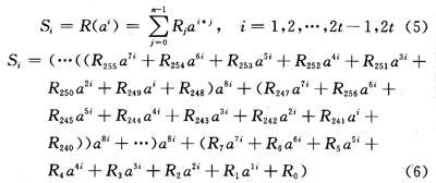
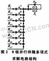
In formula (6), R255=0; i=1, 2, ..., 2t-1, 2t. The circuit structure is shown in Figure 2.
2.2 Solving the key equations
The ME algorithm is used to solve the key equations in this design. The BM algorithm has a feedback structure and is not suitable for a pipeline structure, while the ME algorithm can use a pipeline structure. The algorithm is described as follows:
![]()
Where S(x) is the adjoint polynomial of the input.
The ME algorithm is an iterative algorithm, the purpose of which is to find the i-th order remainder Ri(x), and the corresponding polynomials ri(x) and Li(x) satisfy:
ri(x)A(x)+Li(x)S(x)=Ri(x)(8)
When the order of the i-th order remainder Ri(x) is less than t, the iterative algorithm ends. At the end of the algorithm, Ri(x) is the error characteristic polynomial ω(x), and Li(x) is the error position polynomial δ(x).
The operation performed by the ME algorithm at each iteration is:

For detailed derivation, please refer to references [8-9].
The single-stage iterative circuit structure is shown in FIG3 .
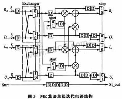
It can be seen from the derivation of the ME algorithm that when the ME algorithm is implemented using a pulsating circuit structure, the order of the R(x) polynomial can be reduced by one order by using at most two levels of iterative circuits. Therefore, the pulsating circuit structure uses a 32-level pipeline structure circuit to ensure that the iterative algorithm completes convergence and obtains the final result. The circuit structure is shown in Figure 4.
 [page]
2.3 Qian Search and Forney Algorithm
The Qian search module receives the error position polynomial signal δ(x) from the KES module, uses the Qian search algorithm to check whether the sign bits are erroneous one by one, and outputs the error position and the sum of the odd terms of the error position polynomial for the EE module to calculate the error pattern and correct the error.
Assume that the error position polynomial δ(x) can be expressed as the sum of odd terms and even terms:
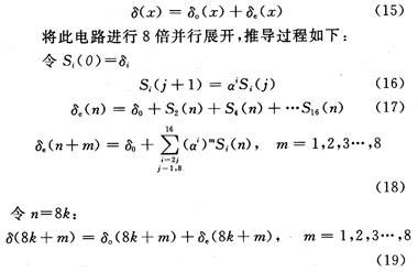
The parallel search circuit substructure is shown in FIG5 . In the figure, m represents the number of parallel modules, m=1, 2, …, 8. All multipliers are constant multipliers, and the 8-fold parallel structure is composed of 8 identical structures shown in FIG5 .
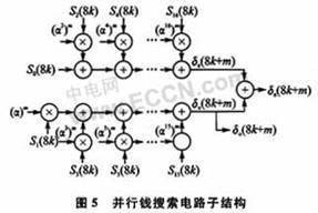
The EE (error value calculation) module calculates the error pattern based on the δodd(x) output by the CS module and the ω(x) output by the KES module.
![]()
The EE module needs to solve w(ai). The circuit structure derivation process is the same as the process of solving δ(ai), and the circuit structure is basically the same, so I will not repeat it here.
3 Simulation Verification and Synthesis
The decoder is divided into modules using a top-down design process, and the RTL code is written using Verilog HDL. Then, the test code is written and simulated using Mentor's ModelSim SE 6.1b simulation verification tool. The simulation results are shown in Figure 6, and the decoder can correctly implement the decoding function.
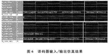
Since this decoder can correct 16 errors and cannot correct more than 16 errors, two types of decoding input samples are used in simulation: one type of sample does not exceed 16 errors, and the other type of sample exceeds 16 errors. The simulation results show that this decoder can decode normally with samples not exceeding 16 errors.
The decoder was synthesized and optimized on Quartus II 8.0, using the EP2C15AF256C8 chip of Altera's Cyclone series as the target device. The decoder's operating clock frequency can reach 85 MHz, the data throughput can reach 5 440 Mb/s, the number of logic cells occupied is 13 947 (a total of 14 448 on the chip, the occupancy rate is 97%), and the RAM occupies 16 698 bits (a total of 239 616 bits on the chip, the occupancy rate is 7%). The decoder performance comparison is listed in Table 1.

Compared with reference [4], the decoder adopts a parallel structure, while increasing the hardware resources by less than 3 times, the throughput-to-clock ratio (throughput/clock) is increased by 8 times, and the decoding delay is shortened by 3/4. Compared with reference [5], the decoder adopted in this paper increases the hardware resources by less than 3 times, and increases the throughput-to-clock ratio by 8 times. Since reference [5] adopts a serial decoding structure, the parallel pipeline decoding structure adopted in this paper reduces the decoding delay by 19/20 compared with the serial decoding structure.
Previous article:PSoC Express enables transparent, code-free PSoC application development
Next article:Addressing High-Speed Board Layout Challenges in FPGA/SDI Subsystems
- Popular Resources
- Popular amplifiers
-
 Siemens PLC Programming Technology and Application Cases (Edited by Liu Zhenquan, Wang Hanzhi, Yang Kun, etc.)
 -
 Intelligent computing systems (Chen Yunji, Li Ling, Li Wei, Guo Qi, Du Zidong)
 -
 MCU C language programming and Proteus simulation technology (Xu Aijun)
 -
 Practical training guidance for new electrician technology (Wu Qihong, Jiang Jian, Xu Kungang, Zhang Hong)
- Huawei's Strategic Department Director Gai Gang: The cumulative installed base of open source Euler operating system exceeds 10 million sets
- Analysis of the application of several common contact parts in high-voltage connectors of new energy vehicles
- Wiring harness durability test and contact voltage drop test method
- Sn-doped CuO nanostructure-based ethanol gas sensor for real-time drunk driving detection in vehicles
- Design considerations for automotive battery wiring harness
- Do you know all the various motors commonly used in automotive electronics?
- What are the functions of the Internet of Vehicles? What are the uses and benefits of the Internet of Vehicles?
- Power Inverter - A critical safety system for electric vehicles
- Analysis of the information security mechanism of AUTOSAR, the automotive embedded software framework
 Professor at Beihang University, dedicated to promoting microcontrollers and embedded systems for over 20 years.
- Innolux's intelligent steer-by-wire solution makes cars smarter and safer
- 8051 MCU - Parity Check
- How to efficiently balance the sensitivity of tactile sensing interfaces
- What should I do if the servo motor shakes? What causes the servo motor to shake quickly?
- 【Brushless Motor】Analysis of three-phase BLDC motor and sharing of two popular development boards
- Midea Industrial Technology's subsidiaries Clou Electronics and Hekang New Energy jointly appeared at the Munich Battery Energy Storage Exhibition and Solar Energy Exhibition
- Guoxin Sichen | Application of ferroelectric memory PB85RS2MC in power battery management, with a capacity of 2M
- Analysis of common faults of frequency converter
- In a head-on competition with Qualcomm, what kind of cockpit products has Intel come up with?
- Dalian Rongke's all-vanadium liquid flow battery energy storage equipment industrialization project has entered the sprint stage before production
- Allegro MicroSystems Introduces Advanced Magnetic and Inductive Position Sensing Solutions at Electronica 2024
- Car key in the left hand, liveness detection radar in the right hand, UWB is imperative for cars!
- After a decade of rapid development, domestic CIS has entered the market
- Aegis Dagger Battery + Thor EM-i Super Hybrid, Geely New Energy has thrown out two "king bombs"
- A brief discussion on functional safety - fault, error, and failure
- In the smart car 2.0 cycle, these core industry chains are facing major opportunities!
- The United States and Japan are developing new batteries. CATL faces challenges? How should China's new energy battery industry respond?
- Murata launches high-precision 6-axis inertial sensor for automobiles
- Ford patents pre-charge alarm to help save costs and respond to emergencies
- New real-time microcontroller system from Texas Instruments enables smarter processing in automotive and industrial applications
- Principles of Adaptive Filters (5th Edition)
- 10-channel logic analyzer based on VGA display.pdf
- TFTP network burning system
- Introduction to the estimation method of the remaining capacity SOC of lithium batteries
- [RVB2601 Creative Application Development] Ultrasonic pressure-sensitive buttons based on RISC-V processor
- First of all, the 9 boards sent by National Technology have arrived. It's so fast.
- There is no year-end bonus this year.
- Pingtou Ge RRVB2601 Review: Unboxing, Hardware Analysis and Environment Setup
- OrangePi Zero GPIO Control
- PIC32MX250F128B please help?

 Siemens PLC Programming Technology and Application Cases (Edited by Liu Zhenquan, Wang Hanzhi, Yang Kun, etc.)


 京公网安备 11010802033920号