In recent years, the world economic situation and energy development pattern have undergone major changes. All countries are concerned about energy issues and are worried that the large-scale use of conventional energy will threaten the living environment of mankind. In order to implement sustainable development, many countries have invested a lot of manpower and material resources in the development and utilization of new energy. The 21st century will enter a new lighting era represented by LED. Due to different geographical conditions, the distribution of solar and wind resources is different. In order to achieve the maximum utilization of wind and light, a wind-solar complementary system is adopted to realize the input of wind-solar complementary power generation as the input of the LED driver circuit. However, the performance of most current drive circuits is unstable. The LED driver power supply still has problems such as poor conversion efficiency, low power factor, poor output current stability, and life that cannot match LED. It has become a bottleneck restricting the further promotion and application of LED lighting devices. The LED driver circuit based on LF-F301 designed in this paper improves these shortcomings. It is based on the improvement of the wind-solar complementary power generation system. In the whole system, the electric energy generated by the wind turbine and the photovoltaic system is provided to the LED street lamp, and the insufficient part is provided by the power frequency power grid. The circuit is connected to the power frequency power grid for a long time, and by optimizing the switch combination, it can be applied in more occasions.
1. Drive circuit design
1.1 LED driving conditions
The rapid development of LED energy-saving lamps has made the design of LED drive circuits more stringent. The entire circuit must not only be safe and low-power, but also have a constant current characteristic, that is, when the power supply voltage changes by 15%, the output current changes by no more than 10%. This is the only way to ensure a higher energy utilization efficiency of the LED drive circuit.
1.2 Driving circuit characteristics
This drive circuit uses a constant current power drive method and is designed for T10 LED lamps. It can be used not only in downtown areas, industrial parks and university campuses, but also in remote areas such as isolated islands and villages, and has broad market application prospects. At the same time, the entire circuit adopts a special switch control method, which makes it have the advantages of high efficiency, energy saving and environmental protection. After research and physical circuit measurement, the drive circuit has the following characteristics: operating frequency 50-60 Hz; power 24 W; wide input voltage AC 110-265 V/50-60 Hz; output current 0.24A; output voltage: 36 V≤Uout≤0.6 Uin; volume 175 mm×18 mm×11 mm; DC 50 V~80V. These parameters ensure that the LED drive circuit is safe and stable when used, making it have the characteristics of high constant current accuracy and good electromagnetic compatibility.
1.3 Driving circuit design
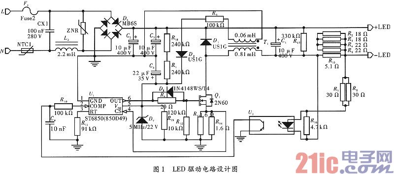
The schematic diagram of the driving circuit is shown in Figure 1. Through the bridge rectifier, the current is directly sent to the positive pole of the LED load, then through the negative pole, through the transformer to the transistor Q1, and finally through the bridge rectifier. This is the main loop of the load circuit current. When there is no load, R17 acts as the load of the protection circuit to ensure that the circuit will not short-circuit. C1 plays the role of filtering and balancing the voltage across the load. D1 is a current storage diode to ensure the normal operation of the transformer. The lower half of the circuit diagram is a feedback regulation circuit composed of two chips and Q1. Q1 can send high-frequency current to the transformer according to the changes in U1. When the load current is overloaded, the current will reach U2 through R7 and R8, causing the diode on the right side of U2 to heat up, resulting in a decrease in the voltage on the left side of U2, and at the same time feedback to U1. U1 adjusts the voltage and frequency control circuit to make the system circuit output a constant current.
2 Analysis of LF-F301 driving circuit principle
2.1 Working Module
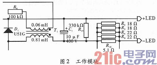
As shown in Figure 2, this circuit outputs appropriate current through the transformer. When there is an LED load, the circuit passes appropriate current and frequency to make the LED work normally; when there is no load, there is still energy remaining in the transformer, which needs to be released. At this time, the circuit composed of R17 and the like can slowly release the electrical energy in the transformer. However, when the current suddenly decreases, an induced electromotive force will be generated in the transformer, which will generate a higher reverse voltage and may break down the device. In order to overcome this problem, a freewheeling diode D1 is connected in parallel at both ends of the coil, and R15 is connected in series at the output end of the circuit, and R2, R3, R4, and R6 are connected in parallel at both ends of R15. R15 has a voltage reduction effect and can provide voltage for the feedback circuit. Since R15 bears a large power and is easy to burn out, a parallel equivalent resistor consisting of R2, R3, R4 and R6 is prepared, so that the power borne by each resistor becomes smaller, which can reduce maintenance costs while increasing the service life.
2.2 Sampling Module
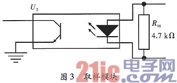
As shown in FIG3 , the sampling current passes through the sensor U2 to convert the current signal into a voltage signal and output it to pin 2 of the chip U1 .
2.3 Control Module
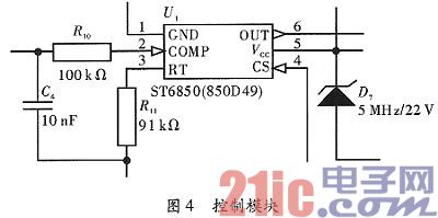
As shown in Figure 4, the circuit obtains a stable 22 V voltage through T1 and D7 to supply the chip. The chip samples the input through pin 2, and C4 controls the frequency and voltage of the circuit.
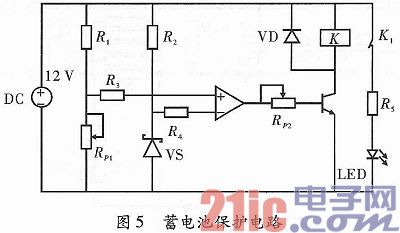
3. Battery protection circuit design
Reasonable battery charging and discharging can not only extend the battery life, but also improve the stability of the entire circuit system. Therefore, it is necessary to design a protection circuit to ensure that the battery can be charged and discharged within a certain voltage range. This project uses a 3-stage cascaded 12 V lead-acid battery. Since the overcharge circuit and the over-discharge circuit are similar, this article only gives the over-discharge circuit of the battery, as shown in Figure 5. When the power supply voltage is normal, adjust the potentiometer RP1 so that the potential of the amplifier's in-phase input terminal is slightly higher than the potential of the inverting input terminal. At this time, the amplifier outputs a low level, VT is cut off, and the circuit works normally. When the power supply voltage is 10.5 V, the potential of the inverting input terminal is greater than the potential of the in-phase input terminal, the amplifier will output a high level, adjust RP2, and turn on VT. At this time, the load is disconnected from the power supply.
4 Circuit switch design
The basic principle of the light-controlled switch is the photosensitivity effect. When the light reaches a certain value, the switch is turned on, otherwise it is automatically turned off. The time-controlled switch turns the circuit on or off according to the set time. However, when the light-controlled switch is used in the field of lighting control, even if the light sensor is placed in a more appropriate position, the light intensity collected in the morning and evening is unstable. If the output ends of the light-controlled switch and the time-controlled switch are connected in series, the light sensor measures the light intensity of the external environment, and the timer gives the required time range, the circuit can be better controlled to shut down, which not only saves energy but also extends the service life of the LED lamp.
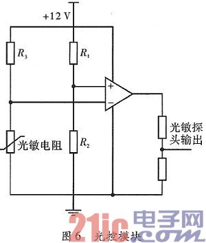
4.1 Light control module
It consists of a photoelectric conversion module and a photoresistor. Photoelectric conversion is achieved by a comparator. When the light intensity sensed by the photosensitive probe is not strong, the comparator will output a high potential, otherwise it will output a low potential. The specific circuit is shown in Figure 6. R1 shares the circuit voltage. According to the external environmental conditions, select the appropriate resistor R2 to control the voltage value of the positive input in the comparator so that it can be used as the reference voltage for the comparator to work; R3 plays a role in protecting the photoresistor and dividing the voltage. The resistance value of the photoresistor changes with the change of the external light intensity, so that the light signal can be converted into a voltage signal, which is connected to the inverting input of the comparator as the signal voltage. Compare the voltages of the two input terminals. If the signal voltage is small, the comparator outputs a high level, otherwise the comparator outputs a low level. This achieves the design requirements of outputting a low level under bright conditions and a high level under dark conditions.
4.2 Time Control Module
The time control module is based on a timer. When the light control module outputs a high level, the time control module enters the working state, which is divided into three stages:
(1) The light intensity gradually decreases, and the LED light is controlled to achieve half-light lighting.
(2) During peak traffic hours, LED lights are controlled to provide full-light illumination.
(3) In the second half of the night, control the LED lights to half-light.
5 Conclusion
The wind-solar complementary circuit driving LED is developing rapidly and has a wide range of application environments. This article explains the application significance and prospects of the driving circuit, analyzes the technical requirements of the driving circuit, and designs the LED power driving circuit. According to the requirements of the driving circuit, while improving the circuit switch, the battery charging and discharging protection circuit is designed, which improves the working efficiency of the entire circuit and achieves the purpose of energy saving and environmental protection.
Previous article:Set-top box descrambling technology
Next article:Intelligently controlled external notebook radiator
- Popular Resources
- Popular amplifiers
- Huawei's Strategic Department Director Gai Gang: The cumulative installed base of open source Euler operating system exceeds 10 million sets
- Analysis of the application of several common contact parts in high-voltage connectors of new energy vehicles
- Wiring harness durability test and contact voltage drop test method
- Sn-doped CuO nanostructure-based ethanol gas sensor for real-time drunk driving detection in vehicles
- Design considerations for automotive battery wiring harness
- Do you know all the various motors commonly used in automotive electronics?
- What are the functions of the Internet of Vehicles? What are the uses and benefits of the Internet of Vehicles?
- Power Inverter - A critical safety system for electric vehicles
- Analysis of the information security mechanism of AUTOSAR, the automotive embedded software framework
 Professor at Beihang University, dedicated to promoting microcontrollers and embedded systems for over 20 years.
- LED chemical incompatibility test to see which chemicals LEDs can be used with
- Application of ARM9 hardware coprocessor on WinCE embedded motherboard
- What are the key points for selecting rotor flowmeter?
- LM317 high power charger circuit
- A brief analysis of Embest's application and development of embedded medical devices
- Single-phase RC protection circuit
- stm32 PVD programmable voltage monitor
- Introduction and measurement of edge trigger and level trigger of 51 single chip microcomputer
- Improved design of Linux system software shell protection technology
- What to do if the ABB robot protection device stops
- Huawei's Strategic Department Director Gai Gang: The cumulative installed base of open source Euler operating system exceeds 10 million sets
- Download from the Internet--ARM Getting Started Notes
- Learn ARM development(22)
- Learn ARM development(21)
- Learn ARM development(20)
- Learn ARM development(19)
- Learn ARM development(14)
- Learn ARM development(15)
- Analysis of the application of several common contact parts in high-voltage connectors of new energy vehicles
- Wiring harness durability test and contact voltage drop test method
- [Sipeed LicheeRV 86 Panel Review] 15. lvgl calendar control and weather display
- Can RTthread be ported to nrf51822?
- A bug solution for CH548/CH549 ADC routine
- [Project source code] BMP2mif file software, convenient for using ROM to store image data and display
- I want to control the on and off of NMOS through a 3.3V microcontroller
- Domestic FPGA brand Anlu
- The load is a 3000W heating plate, controlled by two 16A relays
- "Detailed Explanation of Embedded Linux System Development Technology--Based on ARM (Full Version)" e-book free
- Essential controlSUITE Software Suite for C2000 Microcontrollers
- [National Technology N32 MCU Development Package] --N32G031 Series


 LM2903PW


 京公网安备 11010802033920号