1. Introduction
NAND FLASH has become the mainstream product in current storage applications due to its large storage capacity, small size, fast read and write speed, and simple peripheral circuits. However, the write operation of NAND FLASH is quite special. When storing data, the storage command and storage address must be written first, and no operation can be performed on it during programming. The traditional acquisition with the microcontroller as the core uses the query method to program NAND FLASH, which is not only complicated to operate, but also slows down the storage speed.
For this purpose, a high-speed storage array based on DMA transmission is designed. The DMA method is used to realize the transmission of commands and addresses, and the pipeline storage process is realized, which speeds up the storage speed. In addition, the system uses FPGA as the platform, has high integration, and has flexible bus width, which broadens the application environment of the storage array.
2. System structure
The data storage system structure is shown in Figure 1, which includes the following three parts:
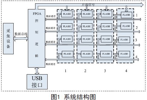
(1) FPGA, the core of the data storage system, has high integration and low power consumption. It is embedded with a soft processor core MICROBLAZE with a flexible bus structure and strong parallel processing capabilities. It also has a user-defined IP core that can control the flash array and correctly store data. It can also upload the data stored in the array to a computer for post-processing.
(2) Storage array: The system adopts a 4×4 array and is built with K9NBG08U5A from SAMSUNG. When building a flash array, all FLASH use the same control signal; the chip select signals of the FLASH in the same column are the same, but the data channels are different; the chip select signals of the FLASH in the same row are different, but the data channels are the same.
(3) USB interface: The host computer and the storage system interact through the USB interface. The host computer transmits commands and configuration information to the FPGA through the USB interface, so that the MICROBLAZE inside the FPGA performs the corresponding operations. When reading back data, the data is transmitted back to the host computer through the USB interface. This design uses FIDI's FT245R as the USB interface chip for communication between the host computer and the FPGA. Using the D2XX driver provided by FIDI, the fastest transmission rate is up to 1MBps.
3.DMA design and implementation
The function of DMA is to control the operation of the flash array to achieve fast data storage. Its design mainly includes two parts: DMA mode write command and address, and the realization of pipeline operation process. DMA mode write command and address is to use hardware method to release the command code and address required for flash array programming to the data bus in time sequence, saving the time wasted when the microcontroller queries; pipeline operation process is DMA's use of the waiting time of the flash array programming stage, which improves the storage speed.
3.1 DMA mode write command and address
When performing storage operations on FLASH, the programming start command should be written to FLASH first, followed by the valid block storage address and 2K bytes of data for five cycles, and finally the end programming command should be written. The time spent on transmitting commands and addresses using DMA is lower than that of microcontroller query, which improves the storage speed. Since the system flash array is small in size, a fully correlated invalid block management method can be used, which has simple control and easy algorithm implementation. The information of the invalid block is cached in the address FIFO in advance and read by DMA when the data is stored. In addition, the programming command code of each NAND FLASH is the same, so when operating each column of flash memory, the data on each FLASH IO port is the same. The DMA write command and address are shown in Figure 2. The same address and command are first juxtaposed together, then sent to the data bus through DMA, and finally allocated to each FLASH I/O port.
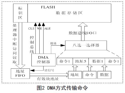
The function of the eight-select-one circuit in Figure 2 is to put the storage data, commands, and addresses on the IO bus of FLASH according to the operation sequence of the flash, and the channel selection is controlled by DMA. At the same time, the corresponding control signals ALE, CLE, WE, etc. become valid levels to realize the writing of commands, data, and addresses.
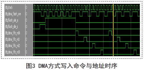
This part of the timing simulation is shown in Figure 3. Signal line 1 is a clock signal with a frequency of 50MHz; signal line 2 is the FLASH write signal; signal line 3 is the ALE signal line. When it is high, the address written to the FLASH will be latched into the address register; signal line 4 is the CLE signal. When it is high, the command written to the FLASH will be latched into the command register; the remaining signals are signals for reading data FIFO.
3.2 DMA pipeline operation process
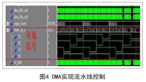
The storage operation of K9NBG08U5A for valid data includes the loading stage and the programming stage. During the programming stage, FPGA cannot operate FLASH. Therefore, for a single-chip FLASH memory, the time of the programming stage is wasted, which is not conducive to fast storage. For this reason, the time division multiplexing method can be used to store data. The specific implementation method is to first load the data to the Nandflash of the first column. After the data is loaded, the first column Nandflash will then enter the automatic programming state and immediately load the second column FLASH. The data is loaded in this cycle until the last piece is loaded and then returns to the first piece. In this way, the time of the programming stage is fully utilized to improve the storage speed. This process is also called pipeline operation.
In order to realize the pipeline storage method, this paper also uses the DMA controller to realize the chip select of FLASH. As shown in Figure 4, flash_ce_s represents the chip select signal of each column of flash, where the low level represents the effective loading of flash. It can be seen from the figure that the DMA controller loads the flash in sequence, realizing the operation process of the pipeline.
4. System Verification
This design designs a counter with a counting clock of 16MHZ in the user logic. Every time the counting clock comes, the data is cached in four FIFOs and stored in the flash array system through DMA. The data is read back through the host computer, as shown in Figure 5.
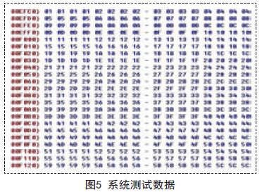
It can be seen from the figure that the 4 consecutive bytes of data are the same, and they come from the same count of data in the 4 cache FIFOs. At the same time, the data is incremented by one every 4 bytes, that is, there is no data loss. It can be seen that the system's DMA controller can realize the fast and correct storage of data in the flash array.
5. Conclusion
This paper proposes a design scheme of data storage array system based on DMA based on the rapid storage of massive data in the measurement and control system. It is a SOPC system built on FPGA platform, containing soft-core processor Microblaze and user-defined IP including DMA controller. Through experiments, it is verified that the DMA controller designed in this scheme realizes the transmission of programming commands and addresses of flash array, as well as pipeline programming of storage array, which improves the speed of traditional storage test system composed of CPLD and single-chip microcomputer.
Previous article:Research on the network security protection system model and its key technologies based on APT intrusion
Next article:Design of experimental equipment sharing platform based on RFID technology
Recommended ReadingLatest update time:2024-11-23 08:04

- Popular Resources
- Popular amplifiers
-
 Microcomputer Principles and Interface Technology 3rd Edition (Zhou Mingde, Zhang Xiaoxia, Lan Fangpeng)
 -
 Automotive Electronics S32K Series Microcontrollers: Based on ARM Cortex-M4F Core
 -
 LPC1700 Chapter 31 General Purpose DMA
 -
 ARM Cortex-M4+Wi-Fi MCU Application Guide (Embedded Technology and Application Series) (Guo Shujun)
- "Cross-chip" quantum entanglement helps build more powerful quantum computing capabilities
- Why is the vehicle operating system (Vehicle OS) becoming more and more important?
- Car Sensors - A detailed explanation of LiDAR
- Simple differences between automotive (ultrasonic, millimeter wave, laser) radars
- Comprehensive knowledge about automobile circuits
- Introduction of domestic automotive-grade bipolar latch Hall chip CHA44X
- Infineon Technologies and Magneti Marelli to Drive Regional Control Unit Innovation with AURIX™ TC4x MCU Family
- Power of E-band millimeter-wave radar
- Hardware design of power supply system for automobile controller
 Professor at Beihang University, dedicated to promoting microcontrollers and embedded systems for over 20 years.
- Intel promotes AI with multi-dimensional efforts in technology, application, and ecology
- ChinaJoy Qualcomm Snapdragon Theme Pavilion takes you to experience the new changes in digital entertainment in the 5G era
- Infineon's latest generation IGBT technology platform enables precise control of speed and position
- Two test methods for LED lighting life
- Don't Let Lightning Induced Surges Scare You
- Application of brushless motor controller ML4425/4426
- Easy identification of LED power supply quality
- World's first integrated photovoltaic solar system completed in Israel
- Sliding window mean filter for avr microcontroller AD conversion
- What does call mean in the detailed explanation of ABB robot programming instructions?
- STMicroelectronics discloses its 2027-2028 financial model and path to achieve its 2030 goals
- 2024 China Automotive Charging and Battery Swapping Ecosystem Conference held in Taiyuan
- State-owned enterprises team up to invest in solid-state battery giant
- The evolution of electronic and electrical architecture is accelerating
- The first! National Automotive Chip Quality Inspection Center established
- BYD releases self-developed automotive chip using 4nm process, with a running score of up to 1.15 million
- GEODNET launches GEO-PULSE, a car GPS navigation device
- Should Chinese car companies develop their own high-computing chips?
- Infineon and Siemens combine embedded automotive software platform with microcontrollers to provide the necessary functions for next-generation SDVs
- Continental launches invisible biometric sensor display to monitor passengers' vital signs
- MSP430F5529LP Example
- Ask for advice - paid 6678 download code and start via USB
- Operational amplifier parameter analysis and LTspice application simulation" Reading notes 1 Remember the gap between ideal and reality
- Beijing Embedded Software and Hardware Recruitment
- Automotive FPGA Solutions
- High frequency transformer, low frequency transformer, pulse transformer
- NBIoT and LoRa technology detailed explanation and competitive situation analysis
- Selling an ATRCB256RFR2-XPRO Wireless Evaluation Kit
- Intersil Handheld RFID Reader Solutions
- Book now to get a gift: Live broadcast on April 9, MIPI C-PHY? Understand it, learn it, and design it

 Microcomputer Principles and Interface Technology 3rd Edition (Zhou Mingde, Zhang Xiaoxia, Lan Fangpeng)


 京公网安备 11010802033920号