Traditional NAND often faces inefficiencies in power, performance and cost. NEO Semiconductor announced that it has recently obtained some patents in the field of X-NAND that can overcome these limitations.
Since NAND was commercialized and mass-produced in the early 1990s, developers have been looking for ways to increase performance while reducing the cost per bit.
NEO Semiconductor, a company that makes 3D NAND flash memory, recently patented a technology called "X-NAND" that it says can address some of the limitations of traditional NAND technology.
Limitations of NAND Technology
Existing NAND technology faces several obstacles, including:
Single-Level Cell (SLC) Cache Issues
Layer limit
Imperfect page buffer structure
High power consumption
Performance/cost inefficiencies
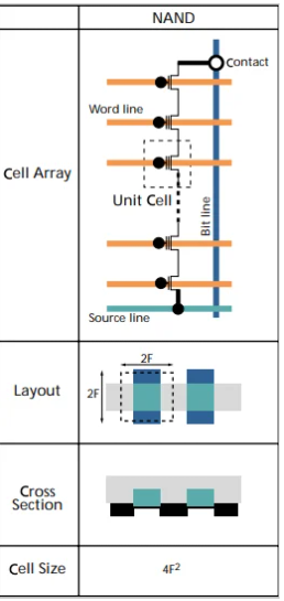
A typical NAND flash memory cell. Image courtesy of Micron
SLC cache problem
One of the reasons why NAND flash is often associated with slower read and write speeds is its traditional SLC cache full problem. Although NAND's migration from single-level cell (SLC) to triple-level cell (TLC) and quad-level cell (QLC) has greatly reduced chip costs and increased density by 33%, the increase in cell levels has had an adverse effect on read and write performance. As a result, this type of flash memory is still unreliable in high-performance applications such as artificial intelligence and 5G.
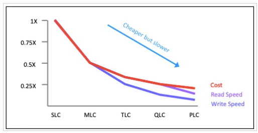
Cost and speed comparison between various memory cells. Image courtesy of NEO Semiconductor
Limited number of layers
To achieve greater read/write bandwidth and higher performance in flash memory architectures, manufacturers typically choose to increase the number of layers. This solution requires connecting the bit lines of each plane to the page buffer, which increases the size of the chip.
Imperfect page buffer architecture
Traditional NAND technology is characterized by an imperfect page buffer structure. This technology requires a connection between a 16KB page buffer and a corresponding 16KB bit line in each plane to perform read/write operations. Therefore, the number of page buffers limits its read/write scale, resulting in low efficiency.
High power consumption
NAND technology has a relatively high power consumption due to its bit line capacitance. Therefore, its operation requires more electricity. Its overall performance is also low, and its manufacturing cost is also low.
What is X-NAND?
NEO Semiconductor intends to solve these problems with its recently patented 3D NAND architecture, also known as X-NAND. This technology is said to achieve the high performance of SLC flash memory and the density of QLC. The company also claims that this innovative technology reduces manufacturing costs while also reducing footprint and optimizing power consumption and cooling capabilities.
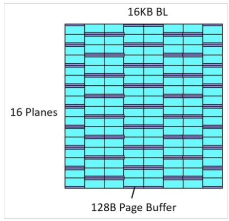
X-NAND flash memory architecture. Image courtesy of NEO Semiconductor
The X-NAND architecture features several upgrades to traditional NAND technology, but there are no major changes to its working principles. NEO Semiconductor claims that NAND manufacturers can implement its technology using existing NAND processes.
Although X-NAND’s cell/array structure and technology are similar to traditional NAND, this new architecture can better support flash performance for machine learning, real-time analytics, network security, 5G, VR/AR and several other applications.
SLC/QLC Parallel Programming
The X-NAND architecture solves the problem of SLC cache fullness through its novel SLC/QLC parallel programming, which allows QLC pages to be programmed at SLC speeds throughout the entire memory capacity. Therefore, this solution is very suitable for data centers and NAS, which require a large number of write systems.
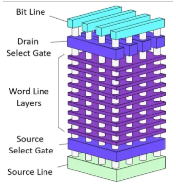
A breakdown of 3D NAND. Image courtesy of NEO Semiconductor
16-layer architecture
Its 16-plane architecture allows for high parallelism at the chip level. Unlike traditional NAND, which is limited to 2 to 4 planes for optimal functionality, X-NAND chips can provide similar or even higher efficiency and parallelism with 4 to 8 NAND chips.
The X-NAND architecture uses 2-16 planes, which significantly increases its performance by 16 times while reducing its chip cost by 33%. This flexibility enables manufacturers to optimize the number of planes of the architecture to meet the performance and chip cost requirements of customers.
According to NEO Semiconductor, the X-NAND QLC architecture has the following improvements compared to traditional NAND QLC.

Comparison of X-NAND and NAND QLC. Image courtesy of NEO Semiconductor
NAND SLC and QLC improvements
Compared to NAND SLC, the company observed the following improvements in random read, random write, sequential read, and sequential write speeds.
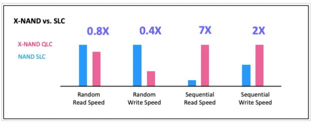
X-NAND compared to NAND SLC. Image courtesy of NEO Semiconductor
The company achieved X-NAND QLC improvements compared to NAND QLC by reducing its bitline capacitance, which resulted in a corresponding reduction in bitline RC delays. Its program verification time accounts for 90% of the program time, making the program three times faster.
Interestingly, increasing its plane count to 16 results in higher read and write bandwidth, and selecting single-latch QLC read and multi-plane QLC procedures has a significant positive impact on sequential read and write speeds.
What Neo Semiconductor's patent means for flash memory
NEO Semiconductor X-NAND includes six different design solutions. This new technology improves the efficiency and cost-effectiveness of multi-bitline read and write operations, including:
Multiple BL write
Multi-plane QLC procedure
Program pause reading
Multiple BL Reading
Single Latch QLC Read
SLC/QLC Parallel Program
Previous article:Memory Cards and Their History in Industrial Applications
Next article:Study on active area shape distortion in advanced DRAM processes
Recommended ReadingLatest update time:2024-11-16 10:51


- Huawei's Strategic Department Director Gai Gang: The cumulative installed base of open source Euler operating system exceeds 10 million sets
- Analysis of the application of several common contact parts in high-voltage connectors of new energy vehicles
- Wiring harness durability test and contact voltage drop test method
- Sn-doped CuO nanostructure-based ethanol gas sensor for real-time drunk driving detection in vehicles
- Design considerations for automotive battery wiring harness
- Do you know all the various motors commonly used in automotive electronics?
- What are the functions of the Internet of Vehicles? What are the uses and benefits of the Internet of Vehicles?
- Power Inverter - A critical safety system for electric vehicles
- Analysis of the information security mechanism of AUTOSAR, the automotive embedded software framework
 Professor at Beihang University, dedicated to promoting microcontrollers and embedded systems for over 20 years.
- Innolux's intelligent steer-by-wire solution makes cars smarter and safer
- 8051 MCU - Parity Check
- How to efficiently balance the sensitivity of tactile sensing interfaces
- What should I do if the servo motor shakes? What causes the servo motor to shake quickly?
- 【Brushless Motor】Analysis of three-phase BLDC motor and sharing of two popular development boards
- Midea Industrial Technology's subsidiaries Clou Electronics and Hekang New Energy jointly appeared at the Munich Battery Energy Storage Exhibition and Solar Energy Exhibition
- Guoxin Sichen | Application of ferroelectric memory PB85RS2MC in power battery management, with a capacity of 2M
- Analysis of common faults of frequency converter
- In a head-on competition with Qualcomm, what kind of cockpit products has Intel come up with?
- Dalian Rongke's all-vanadium liquid flow battery energy storage equipment industrialization project has entered the sprint stage before production
- Allegro MicroSystems Introduces Advanced Magnetic and Inductive Position Sensing Solutions at Electronica 2024
- Car key in the left hand, liveness detection radar in the right hand, UWB is imperative for cars!
- After a decade of rapid development, domestic CIS has entered the market
- Aegis Dagger Battery + Thor EM-i Super Hybrid, Geely New Energy has thrown out two "king bombs"
- A brief discussion on functional safety - fault, error, and failure
- In the smart car 2.0 cycle, these core industry chains are facing major opportunities!
- The United States and Japan are developing new batteries. CATL faces challenges? How should China's new energy battery industry respond?
- Murata launches high-precision 6-axis inertial sensor for automobiles
- Ford patents pre-charge alarm to help save costs and respond to emergencies
- New real-time microcontroller system from Texas Instruments enables smarter processing in automotive and industrial applications
- Brain-electromechanical control robot arm (robot arm for elderly care and disabled assistance)
- Practical Simulation and Testing Technology for Switching Converters
- OK-G2LD-C development board storage read and write speed and network measurement
- Let me tell you about the complicated process of asking Sunny Optical for information yesterday.
- [NXP Rapid IoT Review] + Mobile Synchronizer 5
- I would like to ask what the symbols on the LCD screen of the State Grid electricity meter mean. I have never understood what they mean. Please give me some advice. Thank you.
- bq76930 error in reading temperature value
- EEWORLD University Hall----Live Replay: Detailed Explanation of Ultra-Low Power RSL10 Bluetooth SoC Development Board
- Share the problem and solution of using TB to capture pulse width of MSP430
- When using CPLD to decode AES/EBU audio, the decoded data has spike pulses. What is the reason?

 Improving 3D NAND performance, reliability and yield


 京公网安备 11010802033920号