The IoT spans multiple application areas, and the requirements of design teams can vary greatly depending on the end application area. Power, performance, and cost are priorities in chip design, while application areas such as automotive and aerospace/defense also require functional safety, and in other areas, information security is critical or field upgradability is a requirement.
Verification, prototyping, and software development are commonalities among these areas and design requirements. To allow embedded software development to proceed, early verification techniques were often considered too slow, while abstractions using virtual platforms such as QEMU were sometimes not accurate enough.
FPGA-based prototyping has long been the platform of choice for pre-silicon software development. Hardware emulation in tools like the Cadence Palladium Z1 Enterprise Emulation Platform can scale execution performance from MHz to 100s of MHz at a lower cost, putting it in the hands of more developers on software teams.
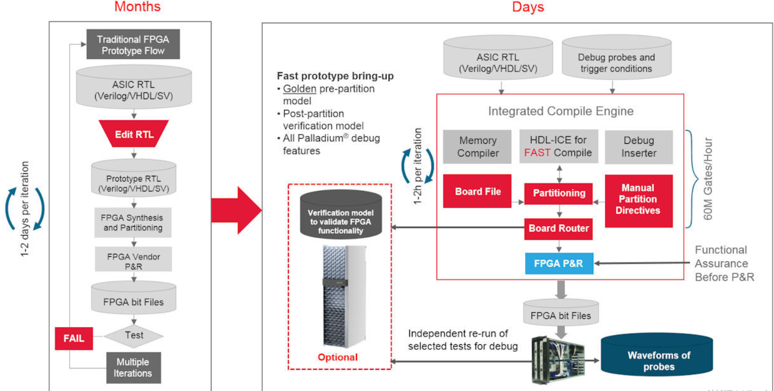
Traditionally, the barrier to FPGA-based prototyping has been the bring-up process, which can sometimes take months before it is available to software developers. The reason for this is the need to remap the ASIC design from its actual silicon into the structure provided by the FPGA, which requires remapping various parts of the design.

Prototype Verification Process
For starters, the memory in the ASIC needs to be mapped to available resources in the FPGA or to a daughter card that has specific additional memory (e.g. DDR). Dealing with clocking the ASIC can be a nightmare, with more than 10 clocks to synchronize in more complex designs on the PCB and FPGA. Partitioning a design across multiple FPGAs is not an easy task and often requires multiplexing multiple signals on the same pin using low voltage differential signaling (LVDS) technology.
Traditionally, larger companies have had prototyping teams that take the RTL versions that the design team is developing and map them into the FPGA. However, as the complexity of designs increases, it becomes increasingly difficult to perform all of the above tasks.
With the Protium S1 FPGA-based prototyping platform, Cadence has redeveloped the prototyping flow and focused on reducing prototyping time from months to weeks or even days by achieving consistency between Palladium Z1 simulation and Protium S1 FPGA-based prototypes, and reusing some of the front-end simulation for prototyping.
Complex manual memory modeling is automated using memory models known from simulation; the compilation flow takes care of partitioning and clock synchronization between FPGAs. Netlists to be mapped into the FPGA fabric can be verified in simulation, saving valuable placement and routing time. Bugs are found approximately 5 times faster in FPGA-based prototypes than in simulation, thus facilitating better debugging capabilities in simulation.
Previous article:Xilinx Launches SmartLynq+ for Versal ACAP, Making It Smarter and More Flexible
Next article:Microchip PolarFire SoC FPGA Now Available at Mouser Electronics
- Popular Resources
- Popular amplifiers
- Why is the vehicle operating system (Vehicle OS) becoming more and more important?
- Car Sensors - A detailed explanation of LiDAR
- Simple differences between automotive (ultrasonic, millimeter wave, laser) radars
- Comprehensive knowledge about automobile circuits
- Introduction of domestic automotive-grade bipolar latch Hall chip CHA44X
- Infineon Technologies and Magneti Marelli to Drive Regional Control Unit Innovation with AURIX™ TC4x MCU Family
- Power of E-band millimeter-wave radar
- Hardware design of power supply system for automobile controller
- Driving Automation Safety and Economic Engineering
 Professor at Beihang University, dedicated to promoting microcontrollers and embedded systems for over 20 years.
- Intel promotes AI with multi-dimensional efforts in technology, application, and ecology
- ChinaJoy Qualcomm Snapdragon Theme Pavilion takes you to experience the new changes in digital entertainment in the 5G era
- Infineon's latest generation IGBT technology platform enables precise control of speed and position
- Two test methods for LED lighting life
- Don't Let Lightning Induced Surges Scare You
- Application of brushless motor controller ML4425/4426
- Easy identification of LED power supply quality
- World's first integrated photovoltaic solar system completed in Israel
- Sliding window mean filter for avr microcontroller AD conversion
- What does call mean in the detailed explanation of ABB robot programming instructions?
- Europe's three largest chip giants re-examine their supply chains
- Breaking through the intelligent competition, Changan Automobile opens the "God's perspective"
- The world's first fully digital chassis, looking forward to the debut of the U7 PHEV and EV versions
- Design of automotive LIN communication simulator based on Renesas MCU
- When will solid-state batteries become popular?
- Adding solid-state batteries, CATL wants to continue to be the "King of Ning"
- The agency predicts that my country's public electric vehicle charging piles will reach 3.6 million this year, accounting for nearly 70% of the world
- U.S. senators urge NHTSA to issue new vehicle safety rules
- Giants step up investment, accelerating the application of solid-state batteries
- Guangzhou Auto Show: End-to-end competition accelerates, autonomous driving fully impacts luxury...
- A brief introduction to commonly used high-frequency electromagnetic field simulation software
- The problem of being unable to sample data when using the 28335 ADC module to sample current
- FPGA_100 Days of Journey_Vending Machine
- About Allegro copper plating
- Draw dice at home
- Altium Designer 21.6.1 7 days of sharing
- How to import CAD files *.dxf/dwg into Altium Designer to make PCB files
- Can such a demand be met?
- MS430G2755 Code transplantation process for MSPBoot
- Company products - rare problems with STM32 MCU ADC

 5962-89636012X


 京公网安备 11010802033920号