Digital signal processors ( DSP ) have been widely used in the control of high-frequency switching power supplies. Taking DSP as the control core of variable-frequency power supplies can achieve flexible and accurate online control with minimal software and hardware. The digital signal processor TMS320LF2407 has the characteristics of general DSP chips and integrates many peripheral circuits on the chip, making it very convenient to realize variable-frequency power supply control. In this paper, the control system adopts the sine pulse width control technology with many engineering applications. This technology has the advantages of simple algorithm, easy hardware implementation, and small harmonics. It can give full play to the high-speed, real-time, and reliability characteristics of DSP. Combined with the corresponding software, some improved algorithms are used to realize SPWM modulation, and the control signal with good quality and arbitrary frequency and amplitude can be output.
1 System Structure
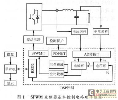
Figure 1 is a hardware block diagram of the basic control circuit of the variable frequency power supply. The variable frequency power supply adopts high-frequency SPWM technology and a universal voltage-type single-phase full-bridge inverter circuit, selects ICBT power modules as switching devices, and adopts a fully digital design for the control circuit.

The output voltage and inductor current are converted into the level required by TMS320LF2407 through the sampling network, and then connected to the A/D conversion port of TMS3201F2407. The required output voltage and frequency values are input through the keyboard, and the SCI module communicates with the DSP. The reference voltage signal of the inverter is obtained, and the actual sinusoidal modulation signal is obtained through the voltage and current regulator. It is intersected with the triangle wave carrier signal generated by the DSP timer, and the drive control signal with a certain dead zone is output. After isolation and amplification by the drive unit, it is sent to the IGBT. The DSP can send the current output voltage and frequency values to the microcontroller and display them on the 8-bit LED. In order to ensure that the power switch and load can be effectively protected in the case of overvoltage, undervoltage, overcurrent (overload), a protection circuit is set in this system. Once a fault occurs, the PDPINT pin is in a low level state, the drive pulse control signal is blocked, and the variable frequency power supply output is cut off.
2 SPWM wave software design
The core of the development of variable frequency power supply is the generation of SPWM wave, which can be realized by software using DSP. The system adopts a dual closed-loop feedback control strategy, the outer loop of which is the output voltage feedback. The voltage regulator generally adopts the PI form, the inductor current feedback constitutes the inner loop, and the current loop is designed as a proportional link. As can be seen from Figure 1, the output voltage signal is directly fed back after conditioning and sampling to generate Vf, and after comparison with the reference sinusoidal voltage Vref, it is adjusted by PI as the given signal Ig of the current inner loop. The error obtained by comparing it with the inductor current feedback value If is adjusted by P, and is used as a modulation wave to intersect with the triangular carrier to generate an SPWM switching signal. In order to facilitate the online debugging of the inverter, the modulation ratio of the generated SPWM wave must be able to be arbitrarily changed within a certain range, and the error is small. From the above, it can be seen that the generation of SPWM wave involves three aspects: obtaining the reference stop-string voltage Vref, realizing the dual closed-loop control of voltage and current, and generating a triangular carrier. Among them, the realization of the triangular carrier is very simple and can be generated by the general timer in the DSP. In this design, the general timer 1 is used, and the value of the period register TIPR in the timer 1 can be determined according to the carrier frequency. The following focuses on the designs and algorithms involved in the first two aspects.
2.1 Generation of reference sinusoidal voltage signal
DSP reads the required voltage frequency and amplitude from the single-chip computer in real time as the reference (given) of the current output voltage. The sine value at the current moment is obtained. The reference sine signal is generated by table lookup. In the digital control system, the sine reference signal is a sine data table, so the sine wave should be made into a table of 0° to 360° according to its expression for reference. In this design, the number of data points in the sine data table is selected as 1024, and its value can be placed in the off-chip data memory. There is a relationship as shown in the figure:
Where: fs is the modulation frequency at the current moment;
t is the sampling time;
N is the Nth pulse in the entire modulation cycle at the current moment.
Since this system is a variable frequency power supply, that is, fS is changing, and the system adopts asynchronous modulation, N also changes with fS. Therefore, the timing time T must be changed in real time to ensure that the number of pulses in the entire cycle is as close to an integer as possible, so as to avoid or reduce the output waveform containing sub-harmonics of the fundamental wave; in addition, the pulse sequence must be changed in real time to ensure that the output voltage value does not have a large jump.
2.1.1 Changing the timing time in real time
Assuming fS = 400 Hz, the frequency suppression ratio Mf is
Since the number of pulses NE in the whole cycle exceeds 1, NE can only be calibrated to Q0, that is, NE can only be an integer, so NE=62, resulting in a difference of 0.5 in the number of pulses, which is reflected in the bridge arm output voltage, with different numbers of pulses in the positive and negative outputs. This will generate sub-harmonics of the fundamental frequency.
If we use the current pulse number NE to infer the switching frequency, we have fc=62x400=24.8kHz. This switching frequency can maximize the guarantee that the number of pulses in the positive and negative modulation cycles is approximately the same. In the design, the working mode of timer 1 is set to continuous increase and decrease counting mode, so
2.1.2 Changing the pulse sequence in real time
When the frequency does not change, the DSP outputs pulses cyclically according to the original output sequence (N=1, 2, ...NE). If the frequency changes in the Nth cycle, the DSP should output pulses according to the new pulse sequence (N′=l, 2, ...NE′).
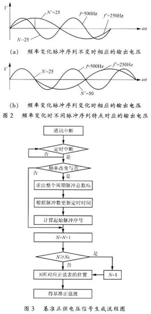
In Figure 2, at the moment N=25, the frequency changes from 500Hz to 250Hz. Since N=25 corresponds to the zero point of the output frequency 500Hz and the positive peak point of the output frequency 250Hz, if the output pulse sequence is not changed, the output voltage phase and voltage value will jump, as shown in Figure 2(a); in Figure 2(b), if the output pulse sequence is changed according to a certain rule, the output voltage phase and voltage value will not jump. In order to ensure that the voltage phase changes to a minimum during the frequency switching process and the output voltage value does not jump significantly, the starting pulse number N′ in the new pulse sequence should be determined according to the following formula, that is,
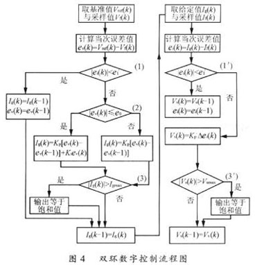
The specific process is shown in Figure 3.

2.2 Dual closed-loop control implementation
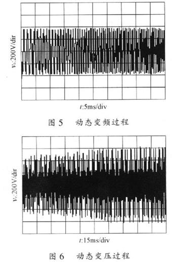
Figure 4 is a flow chart of the voltage and current double closed-loop digital control. In practical applications, considering some specific situations, it is necessary to impose certain restrictions on the digital PI regulation of the voltage regulator and the digital P regulation of the current regulator, and adopt the best control method for different situations. Therefore, some improved algorithms and strategies are adopted at (1), (1'), (2), (3), and (3') in Figure 4, which are briefly introduced below.

In Figure 4, dead zones are set at (1) and (1') because when the output changes slightly, the value of the PWM control register obtained by calculation may also have a small vibration, which will make the system unstable. If an appropriate dead zone range is set, the oscillation caused by this can be eliminated without greatly affecting the output accuracy. According to the actual situation, the minimum input deviation e1 (e1') is set respectively, that is, when |ev(k)|e0, the integral action is cancelled and P control is used. When |ev(k)|≤e0, the integral action is introduced, which not only maintains the integral action but also reduces the overshoot. This greatly improves the control performance of the system.
3 Experimental Results
According to the above basic programming ideas, a general SPWM generation software with an adjustable modulation ratio N can be compiled. As long as the corresponding data is input through the key, an SPWM wave with any output frequency and voltage amplitude can be generated according to the needs of the load. A 5000VA inverter prototype was developed and experiments were carried out. The experimental results show that the output voltage waveform is smooth, the waveform distortion is low, and the THD of the output voltage is ≤2%. In Figure 5, the output voltage frequency is adjusted by changing the given frequency in real time, and the frequency gradually increases from low to high. In Figure 6, the output voltage is adjusted by changing the given voltage amplitude in real time, and the voltage gradually increases from low to high. From the dynamic process of frequency and voltage, it can be seen that the system realizes real-time frequency conversion and voltage conversion.

4 Conclusion
This paper uses DSP as the main control chip to design and implement the digital control of SPWM variable frequency power supply. This method is flexible in control, easy to debug and highly reliable. In the variable frequency power supply using the double closed-loop control strategy, some algorithms suitable for the characteristics of DSP are applied to program the generation of SPWM wave signals that can convert frequency and voltage. The designed method is feasible. Digitalization makes the system highly programmable, so that the system is easier to update and upgrade, and obtains relatively good experimental results.
Previous article:Application of CSE7759 in smart socket and embedded energy metering module
Next article:Design of three-phase SPWM variable frequency power supply based on DSP
- Popular Resources
- Popular amplifiers
- Analysis of the application of several common contact parts in high-voltage connectors of new energy vehicles
- Wiring harness durability test and contact voltage drop test method
- Sn-doped CuO nanostructure-based ethanol gas sensor for real-time drunk driving detection in vehicles
- Design considerations for automotive battery wiring harness
- Do you know all the various motors commonly used in automotive electronics?
- What are the functions of the Internet of Vehicles? What are the uses and benefits of the Internet of Vehicles?
- Power Inverter - A critical safety system for electric vehicles
- Analysis of the information security mechanism of AUTOSAR, the automotive embedded software framework
- Brief Analysis of Automotive Ethernet Test Content and Test Methods
 Professor at Beihang University, dedicated to promoting microcontrollers and embedded systems for over 20 years.
- LED chemical incompatibility test to see which chemicals LEDs can be used with
- Application of ARM9 hardware coprocessor on WinCE embedded motherboard
- What are the key points for selecting rotor flowmeter?
- LM317 high power charger circuit
- A brief analysis of Embest's application and development of embedded medical devices
- Single-phase RC protection circuit
- stm32 PVD programmable voltage monitor
- Introduction and measurement of edge trigger and level trigger of 51 single chip microcomputer
- Improved design of Linux system software shell protection technology
- What to do if the ABB robot protection device stops
- Analysis of the application of several common contact parts in high-voltage connectors of new energy vehicles
- Wiring harness durability test and contact voltage drop test method
- From probes to power supplies, Tektronix is leading the way in comprehensive innovation in power electronics testing
- From probes to power supplies, Tektronix is leading the way in comprehensive innovation in power electronics testing
- Sn-doped CuO nanostructure-based ethanol gas sensor for real-time drunk driving detection in vehicles
- Design considerations for automotive battery wiring harness
- Do you know all the various motors commonly used in automotive electronics?
- What are the functions of the Internet of Vehicles? What are the uses and benefits of the Internet of Vehicles?
- Power Inverter - A critical safety system for electric vehicles
- Analysis of the information security mechanism of AUTOSAR, the automotive embedded software framework
- PIC16F1823 compiles with mplab and reports an error, please help
- Young people seeking employment today
- The most critical part of stm32 id encryption and anti-cracking
- 【GD32307E-START】+RTC electronic clock
- When using PICkit3 to burn the program on PIC32MX250F1828B, it prompts "Program memory is not blank. Faile...
- Analysis of the phenomenon of the teaching module
- Types and Design Ideas of SRAM Sense Amplifiers
- Another layoff! IBM may lay off thousands of employees due to the epidemic!
- Texas Instruments' solutions for sweeping robot systems
- What design solutions does a complete smart home system include?

 ADA10000S3CTR


 京公网安备 11010802033920号