Space-Time Block Coding (STBC) is an effective coding method that reaches or approaches the capacity of MIMO wireless channels. Blind recognition of space-time coding is an area that needs urgent research in the field of communication countermeasures. It can provide the basis and technical support for MIMO system countermeasures and has important research value.
The time-delay correlation algorithm is based on the difference of correlation matrices of different space-time codes under different time delay statistics, and uses step-by-step comparison to achieve blind recognition of space-time coding methods. It has the advantages of high calculation accuracy and good anti-frequency offset effect. This paper proposes a design and implementation of a space-time coding blind recognition scheme based on ADI's DSP chip TigerSHARCTS201S.
1 System Hardware Design
1.1 System Hardware Block Diagram
The system hardware block diagram is shown in Figure 1. It consists of four parts: signal processing, signal acquisition, power supply, and clock. Signal acquisition consists of CPLD and ADC, which are responsible for completing A/D conversion. Signal processing consists of TS201S chip and its peripherals, which are used to store A/D sampled data and perform space-time code blind recognition operations. The power supply module provides the voltage required for normal operation of all other modules. The clock module consists of crystal oscillator and frequency multiplication chip, which provides the clock required by the system.
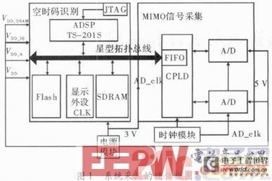
When the system is working, the device is first powered on and initialized, and the user application is loaded from the Flash. Then, the ADC is controlled by the CPLD to collect data, and the DMA interrupt method is used to read the data and perform code recognition operations.
1.2 TigerSHARC TS201S Introduction
TigerSHARC TS201S combines the signal processing performance of ASIC and FPGA with the high programmability and flexibility of instruction set processors, and is suitable for high-performance, large-storage signal processing and imaging applications.
TS201S is divided into two parts: DSP core and I/O interface. Data, address and control information are transmitted through 4 buses. It also provides a fully interruptible programming mode, supports assembly and C/C++ language programming, 32/40-bit floating-point operations and up to 64-bit fixed-point operations. At a clock rate of 600 MHz, it can achieve 4.8 billion multiplication and addition operations per second.
1.3 Power, clock and bus solution design
TS201S and AD7864 have high requirements for power supply. Taking the TS201S core clock of 500 MHz as an example, the accuracy of the four power supplies VDD, VDD_A, VDD_IO, and VDD_DRAM must be controlled within 5%. Therefore, the power supply chip in the system adopts a precision of 1%.
In the clock module, the crystal oscillator generates a 27 MHz clock, which is then passed through the frequency multiplier chip to obtain a 54 MHz clock and enters the CPLD. On the one hand, it is used as the system clock SCLK of TS201S, and on the other hand, it is divided by 12 in the CPLD and used as the working clock signal AD_CLK of AD7864. To prevent coupling interference to the system power supply, the power supply of the crystal oscillator and the frequency multiplier chip should be isolated from the power supply of this board with inductors or magnetic beads.
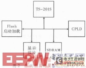
When the system bus is heavily loaded, improper design will limit the bus to work at low frequency or even fail to read data. Since any load change on the ring structure will affect the work of other loads, a star bus structure is used in the design, as shown in Figure 2.
1.4 Signal acquisition scheme design
The signal acquisition module consists of CPLD and two ADCs. The A/D conversion chip uses AD7864 produced by AD Company. It has a conversion accuracy of 12 bits, a maximum throughput of 520 ksample·s-1, a fastest conversion time of 1.65μs, and a sampling and holding time of 0.35μs. In addition, its single power supply and low power consumption characteristics can reach as low as 20 Uw, which can meet the system requirements and simplify the hardware design.
Before signal acquisition, some input pins of AD7864 need to be configured, which can be done by MAX3256, a CPLD product of South Alterta. As shown in Figure 3, CONVST is the enable input pin, which can be set high to control the start of AD7864. CS is the chip select signal, which is valid at low level. RD is the read enable, which is valid at low level. When CS is valid and RD is low, AD7864 is allowed to output the conversion result. At this time, WR must be high. Pins SL1~SL4 are the channel selection input pins of AD7864, which are valid at high level. When H/S SEL is high, it means that the A/D conversion channel will be selected by software, otherwise it means hardware selection. When the conversion is completed, the EOC pin inputs a low level.
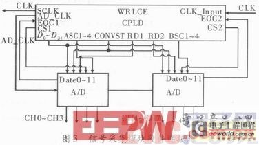
AD7864 adopts time-sharing output mode. The sampling signal comes from the timer/counter of TS201S. Every time the counter is full, the TMROE pin will generate a high level of 4 bus clocks. After inverting this signal in CPLD, it serves as the CONVST signal of AD7864. In data transmission, chip 1 occupies the low-order data line and chip 2 occupies the high-order data line. Time-sharing can prevent bus conflicts.
1.5 Display scheme design
The system uses FLAG PIN external LED as progress display. When the DSP executes different processing progress, it controls the corresponding LED to turn on by changing the level of the FLAG PIN port to indicate the current data analysis step. Figure 4 is a connection diagram of the external LED. Each LED on the FLAG PIN does not affect other FLAG PIN interfaces. A pull-up resistor is used after the LED to connect to VCC.
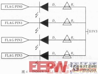
When the system is reset, all FLAG PINs are set to high level, ADC acquisition is completed, DMA interrupt is triggered, data is read from SDRAM, and pre-whitening processing is entered. At this time, FLAG PIN1 is set to low level. According to the algorithm, the time-delay correlation analysis is performed on the whitened data, and the code word table is used to determine the response code type, and FLAG PIN2 and FLAG PIN3 are pulled low respectively.
This method has flexible configuration and simple software. The system uses 4 FLAGPINs to arrange the display. The DSP has sufficient IO interfaces. The hardware resources are fully utilized during the design. At the same time, DMA interrupts are used to effectively improve the efficiency of the CPU, and resource sharing and parallel processing are realized. At the same time, faults are discovered and located in time during the chip operation process.
2 System Software Design
2.1 Principle of Blind Recognition of Space-Time Codes
STBC improves the system transmission performance by performing joint coding in time and space. Therefore, the data sent from different antennas at different times have a certain correlation, and the correlation between different space-time codes is different. Therefore, the correlation can be used to distinguish different code types, thereby identifying the space-time coding pattern.
2.2 Blind recognition method of space-time coding
(1) Pre-whitening. The purpose of pre-whitening is to remove the influence of the channel on the correlation of the received signal. The whitening matrix W is obtained by performing eigenvalue decomposition on the time-sharing correlation matrix P.
, where A-1 is the generalized inverse of the eigenvalue matrix Λ. Multiplying W with the original data will yield the decorrelation matrix Y. (2) Calculating the time-delay correlation. Using the decorrelation matrix Y obtained after pre-whitening the received signal, the time-delay correlation norm is calculated according to the statistical formula

The theoretical time-delay correlation characteristics of the space-time coding matrix are only related to the coding matrix itself. Therefore, the same form as equation (1) can be used to perform matrix multiplication and addition operations on different columns of the coding matrix and take the F norm to characterize it.
From this, we can get the time-delay correlation matrix R(τ) for calculating space-time coding:

Among them, each column of the space-time coding matrix represents a different transmission time, A(u) is the u-th column of the code type A coding matrix, and l is the code type group length. The pre-whitened received signal matrix and the transmitting end coding matrix have the following relationship in the norm of the time-delay correlation function F:

(3) Decision code type. Traverse the candidate code set, calculate the correlation between the received signal and each space-time code in the candidate code set, and take the most correlated code type as the decision code type.
2.3 Software Design
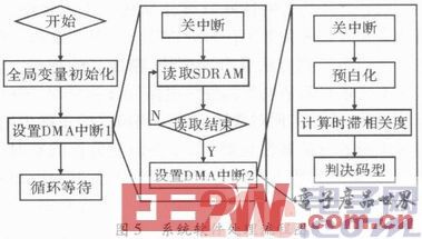
The software system adopts a modular structure design, and the program flow is shown in Figure 5. It includes system startup, configuration of system registers, setting of global variables, and enabling of interrupt control. When the ADC module writes all the sampled data into SDRAM, the CPLD notifies the DSP to trigger DMA interrupt 1, reads the data in SDRAM into the DSP, and after the reading is completed, the DMA triggers interrupt 2 and processes the ADC sampled data: (1) Pre-whitening to remove the influence of the new arrival on the correlation of the sampled data. (2) Calculate the time-delay correlation between the sampled data and each codeword in the candidate set. (3) According to the above calculation results, select the code type that minimizes the time-delay correlation as the decision code type.
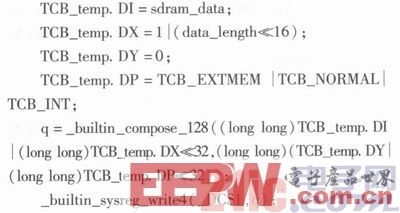
By setting the DMAC register, the direction, channel and mode of DMA can be controlled. The typical key code for data reading is as follows:
The key functions of the data processing part include whitening and time-delay correlation calculation. The data transmission adopts the method of single-dimensional reading and multi-dimensional transmission, that is, the data of multiple antennas are read in sequence according to the antenna order, but when the data is transmitted inside the DSP, the data of multiple antennas are transmitted in time order, and the addressing is manually performed inside the function, which not only meets the algorithm requirements, but also speeds up the data processing speed. The data processing includes a large number of matrix transposition and multiplication and addition operations. The calculation is optimized to the inner product calculation mode, using ALU operation blocks X and Y, and the correlation norm between the two columns of the time-delay matrix is calculated in parallel in each cycle, which saves memory resources, reduces the number of addressing times, and speeds up the calculation speed.
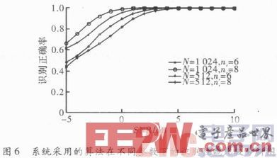
The Matlab performance simulation of this algorithm under different parameters is shown in Figure 6. The longer the sampling data and the more receiving antennas, the better the recognition performance. The actual test proves that it is consistent with expectations, verifying the rationality and correctness of the design.
3 Conclusion
The special hardware and software structure and instruction system of the DSP chip enable it to process various digital signal processing algorithms at high speed. The blind recognition method of space-time coding based on this design has the characteristics of fast speed and high accuracy. At the same time, the system relies on simple external hardware circuit design and reasonable software program design to achieve correct recognition of commonly used space-time coding modes. And the system has good scalability. When it is necessary to identify the latest space-time coding, it only needs to be put into the coding method candidate set and assigned a display interface, without too much change in hardware settings and software programs.
Previous article:Design of DAC expansion circuit for flight control computer based on DSP28335
Next article:Design of Micro-displacement Stepping Motor Control System Based on DSP
- Popular Resources
- Popular amplifiers
- Huawei's Strategic Department Director Gai Gang: The cumulative installed base of open source Euler operating system exceeds 10 million sets
- Analysis of the application of several common contact parts in high-voltage connectors of new energy vehicles
- Wiring harness durability test and contact voltage drop test method
- Sn-doped CuO nanostructure-based ethanol gas sensor for real-time drunk driving detection in vehicles
- Design considerations for automotive battery wiring harness
- Do you know all the various motors commonly used in automotive electronics?
- What are the functions of the Internet of Vehicles? What are the uses and benefits of the Internet of Vehicles?
- Power Inverter - A critical safety system for electric vehicles
- Analysis of the information security mechanism of AUTOSAR, the automotive embedded software framework
 Professor at Beihang University, dedicated to promoting microcontrollers and embedded systems for over 20 years.
- LED chemical incompatibility test to see which chemicals LEDs can be used with
- Application of ARM9 hardware coprocessor on WinCE embedded motherboard
- What are the key points for selecting rotor flowmeter?
- LM317 high power charger circuit
- A brief analysis of Embest's application and development of embedded medical devices
- Single-phase RC protection circuit
- stm32 PVD programmable voltage monitor
- Introduction and measurement of edge trigger and level trigger of 51 single chip microcomputer
- Improved design of Linux system software shell protection technology
- What to do if the ABB robot protection device stops
- Allegro MicroSystems Introduces Advanced Magnetic and Inductive Position Sensing Solutions at Electronica 2024
- Car key in the left hand, liveness detection radar in the right hand, UWB is imperative for cars!
- After a decade of rapid development, domestic CIS has entered the market
- Aegis Dagger Battery + Thor EM-i Super Hybrid, Geely New Energy has thrown out two "king bombs"
- A brief discussion on functional safety - fault, error, and failure
- In the smart car 2.0 cycle, these core industry chains are facing major opportunities!
- The United States and Japan are developing new batteries. CATL faces challenges? How should China's new energy battery industry respond?
- Murata launches high-precision 6-axis inertial sensor for automobiles
- Ford patents pre-charge alarm to help save costs and respond to emergencies
- New real-time microcontroller system from Texas Instruments enables smarter processing in automotive and industrial applications
- HC32F460 Clock System Introduction
- Swagbadge2021 Digital Badge
- Power inductor parameter issues
- How to use arrays in C language for microcontrollers
- Newbies to the forum
- How to read the level of P9~p0 of MAX7317
- Invitation: EEWorld 15th Anniversary Carnival series of activities has begun, it’s great to have you!
- Stock materials, transfer to those in need at low prices.
- Optimal Design of Digital Quadrature Demodulation Receiver Based on FPGA
- uasyncio monitor

 OP215AJ/883C


 京公网安备 11010802033920号