With the extensive development of microwave technology, the electromagnetic environment in space and on the ground is becoming more and more complex. As a kind of public resource, radio spectrum resources need to be effectively allocated and monitored by spectrum management departments. Especially in the case of increasingly crowded frequency bands and increasing natural and man-made interference, it is necessary for spectrum monitoring systems to monitor and detect existing interference so as to take measures to minimize the impact and ensure the rational use of spectrum resources.
The electromagnetic spectrum monitoring analyzer is a detection device that meets the current challenges of electromagnetic signal spectrum detection and has both high resolution and high search speed. The improvement of frequency resolution means that both amplitude detection sensitivity and frequency resolution are improved. Therefore, its high resolution and high-speed scanning characteristics mean that it has strong detection efficiency in the field of electromagnetic signal detection. This system adopts the technical route of high-speed signal storage and processing based on FPGA, DDR2 memory card and multiple DSP, multi-mode multi-window signal detection, and multi-domain signal analysis. It is a high-performance and powerful electromagnetic signal detection and analysis instrument with advantages and wide applications that traditional detection instruments cannot match.
1 System Hardware Solution
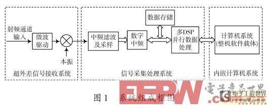
The spectrum monitoring analyzer system consists of three main parts: superheterodyne signal reception, powerful intermediate frequency signal acquisition and processing system, and embedded computer system. Superheterodyne signal reception includes RF channel, microwave drive, local oscillator synthesis, and the signal undergoes three frequency conversions to the sampling intermediate frequency. The intermediate frequency acquisition and processing system is based on the software radio design concept, including intermediate frequency circuit, digital intermediate frequency and storage unit, and multi-DSP parallel signal processing. The embedded computer operating system is Windows XP, which is the carrier of the whole machine software and can be configured with external devices. The whole machine principle block diagram is shown in Figure 1.
2 System Software Design
2.1 Platform and Development Environment
This system intends to use the Wintel architecture, which is the mainstream in the test instrument industry, to build the control platform. The main controller uses a high-performance CoreDuo dual-core processor and selects Windows XP as the software operating platform to fully meet the user's usage habits and data resource sharing needs. The overall software development environment uses the VS2005 integrated development environment and uses Visual SourceSafe for team-based development management.
2.2 Data processing module design
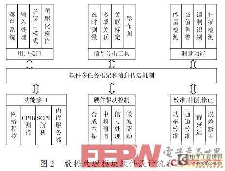
The data processing module mainly collects signals and then sends the data to the computer. The core work of the data processing module is to quantify and collect the signals to be collected. The detailed software design of this module is shown in Figure 2.
2.3 User interface and interface design
This system is designed with two main measurement functions: scanning detection and multi-domain analysis (including modulation identification). For each test function, the parameter test wizard can be activated at a fixed position in the operation interface, and friendly interaction with users can be achieved through drop-down menus, shortcut buttons, traditional menus and numerous dialog boxes. Users can customize parameter test methods and store them as parameter test solutions, which can be directly called for subsequent use, achieving one-click testing and flexible test parameter reporting to better meet different needs.
2.4 Control and data transmission interface design
In this system, the data acquisition and transmission rate is as high as tens of megabytes per second. The whole machine is required to have various communication protocols such as USB, LAN, GPIB, parallel port, serial port, etc., support 1024×768 TFT display and LVDS interface, support configurable printing scheme, support mass/mobile storage devices, and need to realize the control of digital intermediate frequency module, analog circuit module, special peripherals and general peripherals. Among them are high-speed processing devices, mass storage devices, and some functional I/O use slow or serial devices. It is obviously unreasonable to use a single standard bus for interface design. Here, a composite bus form combining PCI, USB, and custom instrument control bus is adopted.
3. Implementation of main system technologies
3.1 High-speed data acquisition PCB design technology
A theoretically perfect system design is difficult to achieve the requirements of the theoretical design when it is implemented. This is because all kinds of interference that exist in reality have an impact on the circuit, and practical problems such as ground wiring, power decoupling, and reflection of signal transmission lines must be handled. The following are some design techniques used in this project to address these problems: avoid straight corners in routing, and use 45° routing or arcs as much as possible; use vias as little as possible, because each via is an impedance discontinuity point; try to widen the width of the power and ground lines, and it is best that the ground line is wider than the power line. Their relationship is: ground line. >Power line>Signal line;The crosstalk between signals is extremely sensitive to the length and spacing of adjacent parallel traces. Therefore, the overall routing directions of signal lines in adjacent routing layers are generally perpendicular to each other. On the same routing layer, the spacing between high-speed signal lines and other parallel signal lines should be increased as much as possible, and the parallel length should be reduced;On the basis of optimizing the layout, the length of high-speed signals should be shortened as much as possible. Controlling the consistency of signal group delay is an important task during wiring;No stubs are used, because any stub is a noise source. If the stub is short, it can be terminated at the end of the transmission line. If the stub is long, the main transmission line will be used as the source, resulting in large reflections and complicating the problem.
3.2 Multi-DSP Interconnection Technology
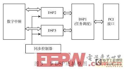
In order to improve the signal processing speed, multiple DSP processors are used, and the DSP model used is AD SP-TS20IS of AD Company . This system uses three high-performance DSPs for high-speed processing, of which two are signal processing DSPs and one is a management DSP. As two signal processing DSPs, they receive the sampling data of the front-end A/D in a time-sharing manner, and then perform digital parallel filter group processing to extract the frequency information, power information, and bandwidth information of the signal. The processing results of the two DSPs are sent to the management DSP. The management DSP is the link between the data processing layer and the data management layer, and is responsible for coordinating the work of the multi-DSP processing system. The multi-DSP connection block diagram used in this system is shown in Figure 3.
3.3 Energy Detection Technology
Threshold setting and calculation are the premise and key to signal energy detection. When the user monitors and analyzes a narrow frequency range, the level threshold method can be used. The level threshold is simple and convenient to set and use as a single level. However, when the frequency band is wide, the level threshold cannot effectively complete the monitoring of smaller level signals when multiple bands are scanned simultaneously. For this purpose, an automatic threshold algorithm is designed (see Figure 4). The automatic threshold automatically calculates the background noise power based on the spectrum data by the software, and distinguishes the noise from the signal by adding an offset value.

4. Implementation of system functions
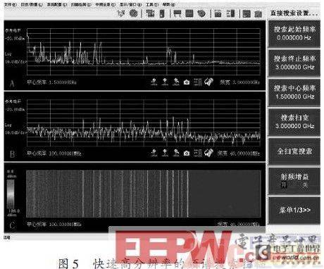
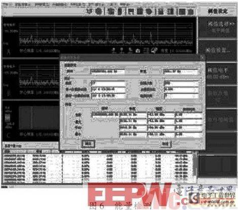
Various functions of the spectrum monitoring analyzer designed in this paper have been realized. Several function implementation interfaces are shown in Figure 5 and Figure 6, which plays an important role in spectrum monitoring.
5 Conclusion
This paper designs a general scheme of spectrum monitoring analyzer, which consists of three main parts: superheterodyne signal reception, powerful intermediate frequency signal acquisition and processing system, and embedded computer system. While designing the overall scheme, several key technologies for realizing this overall scheme are given. Practice has proved that the spectrum monitoring system has the characteristics of high resolution, high-speed search, high-speed storage and processing, and has good application prospects.
Previous article:Speech Data Acquisition and Processing System Based on DSP and MATLAB
Next article:Design of real-time image target search and tracking system based on DSP
- Popular Resources
- Popular amplifiers
- Detailed explanation of intelligent car body perception system
- How to solve the problem that the servo drive is not enabled
- Why does the servo drive not power on?
- What point should I connect to when the servo is turned on?
- How to turn on the internal enable of Panasonic servo drive?
- What is the rigidity setting of Panasonic servo drive?
- How to change the inertia ratio of Panasonic servo drive
- What is the inertia ratio of the servo motor?
- Is it better for the motor to have a large or small moment of inertia?
 Professor at Beihang University, dedicated to promoting microcontrollers and embedded systems for over 20 years.
- LED chemical incompatibility test to see which chemicals LEDs can be used with
- Application of ARM9 hardware coprocessor on WinCE embedded motherboard
- What are the key points for selecting rotor flowmeter?
- LM317 high power charger circuit
- A brief analysis of Embest's application and development of embedded medical devices
- Single-phase RC protection circuit
- stm32 PVD programmable voltage monitor
- Introduction and measurement of edge trigger and level trigger of 51 single chip microcomputer
- Improved design of Linux system software shell protection technology
- What to do if the ABB robot protection device stops
- Detailed explanation of intelligent car body perception system
- How to solve the problem that the servo drive is not enabled
- Why does the servo drive not power on?
- What point should I connect to when the servo is turned on?
- How to turn on the internal enable of Panasonic servo drive?
- What is the rigidity setting of Panasonic servo drive?
- How to change the inertia ratio of Panasonic servo drive
- What is the inertia ratio of the servo motor?
- Is it better for the motor to have a large or small moment of inertia?
- What is the difference between low inertia and high inertia of servo motors?
- [Mill MYB-YT507 development board trial experience] Python displays memory and CPU real-time status 1
- How do RF circuits and digital circuits coexist harmoniously?
- Xiangshan high-performance RISC-V processor
- Issues with converting remaining TI points into chip points
- Development process of eCAN in DSP28335
- Sugar gliders Part ⑩ Sugar glider health monitoring system based on RSL10 - host computer design
- Can someone help me figure out whether this active filter is a voltage-controlled power supply type or a multiple feedback type?
- 【BearPi-HM Nano】NFC test
- Frost has fallen~
- Summary by an expert: Answers to 23 classic questions in power supply development!

 NJM072BE-(T1)


 京公网安备 11010802033920号