1 Control principle of deadbeat control inverter
Deadbeat control is a fully digital control method that uses the high-speed numerical calculation function of a microprocessor through digital instantaneous feedback of status. Figure 1 shows the main circuit of the inverter, which consists of an inverter bridge, LC filter and resistive load. LCR can be expressed by the equation of state:


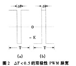
In the inverter system, Uin is the output of the inverter bridge and is an intermediate variable; only the pulse width ΔT is the original control variable. Moreover, the main circuit of the inverter can be considered as a digital-analog hybrid circuit, so it can be analyzed more conveniently using discrete variable state equations. For the circuit shown in Figure 1, Uin can be unipolar or bipolar. If Uin is bipolar as shown in Figure 2, equation (1) can be discretized [ 1 ][2]:

Formulas (2.a) and (2.b) correspond to (a) and (b) in Figure 2 respectively. Take the first row of matrix equations (2.a) and (2.b) respectively, and let, UC(K+1)=U*C(K+1), U*C be the reference sine, the required pulse width can be calculated accordingly. Then , at the beginning of each switching cycle, UC and IC must be detected first (the change of the bus voltage E is small, and it is not necessary to detect it accurately on time ), and then calculate ΔT. Therefore, in a practical system, three sensors and an A/D converter are usually needed to detect the DC bus voltage, output voltage and filter capacitor current. Since A/D conversion and calculation require a certain amount of time, the maximum value of ΔT is limited. It can be seen from Figure 2 that if the output is positive, using Figure 2a, then ΔT ≤ 0.5T. Therefore, there is enough (T-ΔT)/2 time for sampling and calculation.

The output phase of an ordinary PWM inverter has a large difference between no-load and full load. This is because although the output phase phase with the given sine, the phase shift of the LC filter is related to the load. The output phase of the deadbeat control inverter is basically unchanged, and it compensates for the phase delay of the LC filter by adjusting the output phase of the inverter bridge.
2 Implementation of Deadbeat Control Inverter
The third-generation digital signal processor (Digital Signal Processor) TMS320F240 series developed by Texas Instruments has 16-bit high-speed fixed-point arithmetic functions. This type of digital signal processor chip has the following advantages:
(1) Very high processing speed. The single instruction execution cycle is 50ns, that is, 20 million instructions can be executed per second. There is a dedicated 16*16 hardware multiplier in the chip , and it is equipped with an 8-level hardware stack and a four-level pipeline processing structure, which greatly improves the processing speed of digital signals. 544kB high-speed on-chip bidirectional access RAM enables high-speed transmission of on-chip data;
(2) Unique parallel structure. In the traditional von Neumann structure, the program code and data units are uniformly addressed, while the F240 uses an improved Harvard structure. The program area and data area storage units are separated, and instruction fetching and data access can be performed at the same time . This further improves the processing speed;
(3) The rich instruction set provides flexible programming capabilities. Not only can it realize various arithmetic and logical operation functions, but it can also easily complete the information transfer between the program area and the data area;
(4) Highly integrated internal resources. A dedicated event manager (Event Manager) is embedded in the chip, which can easily capture event interrupts and output various PWM waveforms. The chip also integrates peripheral functions such as A/D converters, serial communications, and I/O interfaces , making it very easy to construct a control system and greatly reducing hardware overhead.
Due to the above advantages, the DSP F240 series is particularly suitable for realizing the real-time and high-speed processing requirements required for digital control . Its internal resources include :
(1) Three independent 16-bit hardware timers with 6 working modes; a total of 12 PWM pulses are output, which facilitates the realization of single-phase half-bridge, full-bridge and three-phase full-bridge (dead zone can be set, as well as implementation space Vector PWM control) power electronic converter control;
(2) It has three external hardware interrupts and four external event capture interrupts (Capture). The system has software resources such as RESET reset interrupt , power-down interrupt PDPINT, and non-maskable interrupt NMI, which provide guarantee for the safety of the system. At the same time Special events can be handled promptly;
(3) Two independent 10-bit precision A/D sampling converters, internal clock unit with PLL phase-locked loop, watchdog monitoring unit Watchdog, serial synchronization port SPI and serial asynchronous port SCI, 28 programmable Multiplexed I/O ports, etc.
It can be seen from the above internal resources that the TMS320F240 series DSP does not require much hardware overhead when designing the control system , thereby also improving the reliability of the system.


3 Simulation and experimental results
Under ideal conditions, MATLAB is used to simulate the deadbeat controlled half-bridge inverter. The circuit parameters are: L=1mH, C=20μF , and the switching frequency is 10kHz. DC bus voltage E=300V, output 50Hz, 100V peak AC. Its output waveform is shown in Figure 5.


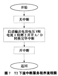
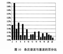
The experiment makes full use of the event manager function and interrupt of TMS320F240 to achieve deadbeat control. Figure 3 and Figure 7 are flow charts of the control main program and interrupt service subroutine. The main program includes initialization (opening and setting corresponding interrupts), startup detection and soft start; the T1 period interrupt service program includes reading the sine table, coefficient calculation and detection of the startup bus voltage, as shown in Figure 4. The T2 underflow interrupt service routine is used to start the detection of U C and I C. The A/D completion interrupt service is used to process the data storage after the bus voltage detection is completed and the calculation of ΔT after the detection of U C and I C , as shown in Figure 6. Figure 8 is the timing distribution diagram of the interrupt service program . 1 and 3 are the T1 period interrupt service program and the T2 underflow interrupt service program respectively; 2 and 4 are the two responses of the A/D completion interrupt service program. Among them, the difference between 1 and 3 is 50μs (0.5T), and the difference between 1, 2 and 3, 4 is 7μs ( the time ). Figures 9 and 10 show the output waveform of the inverter and the proportion of each harmonic. According to Figure 10, the harmonic distortion rate can be calculated to be 0.8%.


References 1 Gokhale KP, Atsuo Kawamura, Hoft RG. Deadbeat Microprocessor Control of PWM Inverter for sinusoidal Output Waveform Synthesis.IEEE-PESC'85.28~36
2 Hua Chihchiang. Two-Lever Switching Pattern Deadbeat DSP Controlled PWM Inverter .IEEE Trans. Power Electron.1995, 10(3): 310~317
3 Yasuhiko Miguchi, Atsuo Kawamura and Richard G.Hoft. Optimal Pole Assignment for Power Electronic Systems.IEEE-PESC'85.74~88
Previous article:Design and implementation of TCP bonding based on FPGA
Next article:Design of DDS digital frequency synthesizer based on CPLD control
Recommended ReadingLatest update time:2024-11-16 19:35


- Huawei's Strategic Department Director Gai Gang: The cumulative installed base of open source Euler operating system exceeds 10 million sets
- Analysis of the application of several common contact parts in high-voltage connectors of new energy vehicles
- Wiring harness durability test and contact voltage drop test method
- Sn-doped CuO nanostructure-based ethanol gas sensor for real-time drunk driving detection in vehicles
- Design considerations for automotive battery wiring harness
- Do you know all the various motors commonly used in automotive electronics?
- What are the functions of the Internet of Vehicles? What are the uses and benefits of the Internet of Vehicles?
- Power Inverter - A critical safety system for electric vehicles
- Analysis of the information security mechanism of AUTOSAR, the automotive embedded software framework
 Professor at Beihang University, dedicated to promoting microcontrollers and embedded systems for over 20 years.
- Innolux's intelligent steer-by-wire solution makes cars smarter and safer
- 8051 MCU - Parity Check
- How to efficiently balance the sensitivity of tactile sensing interfaces
- What should I do if the servo motor shakes? What causes the servo motor to shake quickly?
- 【Brushless Motor】Analysis of three-phase BLDC motor and sharing of two popular development boards
- Midea Industrial Technology's subsidiaries Clou Electronics and Hekang New Energy jointly appeared at the Munich Battery Energy Storage Exhibition and Solar Energy Exhibition
- Guoxin Sichen | Application of ferroelectric memory PB85RS2MC in power battery management, with a capacity of 2M
- Analysis of common faults of frequency converter
- In a head-on competition with Qualcomm, what kind of cockpit products has Intel come up with?
- Dalian Rongke's all-vanadium liquid flow battery energy storage equipment industrialization project has entered the sprint stage before production
- Allegro MicroSystems Introduces Advanced Magnetic and Inductive Position Sensing Solutions at Electronica 2024
- Car key in the left hand, liveness detection radar in the right hand, UWB is imperative for cars!
- After a decade of rapid development, domestic CIS has entered the market
- Aegis Dagger Battery + Thor EM-i Super Hybrid, Geely New Energy has thrown out two "king bombs"
- A brief discussion on functional safety - fault, error, and failure
- In the smart car 2.0 cycle, these core industry chains are facing major opportunities!
- The United States and Japan are developing new batteries. CATL faces challenges? How should China's new energy battery industry respond?
- Murata launches high-precision 6-axis inertial sensor for automobiles
- Ford patents pre-charge alarm to help save costs and respond to emergencies
- New real-time microcontroller system from Texas Instruments enables smarter processing in automotive and industrial applications
- [Synopsys IP Resources] EDA on the cloud makes chip innovation "fast, accurate and stable"
- Internet of Vehicles testing and verification of automotive CAN bus network data
- Which manufacturers are there of domestic battery metering chips?
- Today at 10:00 am | TI Award Live Broadcast [DIY Home Monitoring Edge AI Box]
- [Raspberry Pi Pico Review] - Start compiling the program 2
- USB2.0 Transactions
- Characteristics of voltage-type electrostatic breakdown of MOS tubes
- EEWORLD University Hall----Live Replay: Protecting Clean Water Sources-ADI Water Quality Monitoring Solutions
- Share: How to convert C program from floating point to fixed point
- MicroPython major historical versions

 Building real-time machine learning systems
 Digilent Vivado library
 Circuit Intuition


 京公网安备 11010802033920号