In 2018, the global semiconductor industry reached a scale of 437.3 billion US dollars, of which the semiconductor material scale reached 51.9 billion US dollars. The semiconductor industry in mainland China reached 122 billion US dollars, of which the semiconductor material scale reached 84.4 billion yuan. The semiconductor industry in mainland China accounts for 28% of the global total, and semiconductor materials account for 16% of the global total. The semiconductor industry in Europe, the United States, Japan, South Korea and Taiwan developed earlier, and the global semiconductor materials are still mainly dominated by overseas companies. Domestic companies are still in the initial stage and the degree of participation in the industrial chain is generally low.
At present, the global semiconductor manufacturing industry is in the midst of a historic transformation of shifting to the mainland, and the domestic semiconductor materials industry faces a huge historical opportunity. At present, the localization rate of semiconductor materials in my country is only about 20%. In the future, the domestic semiconductor materials market demand will still grow significantly with the continuous expansion of wafer manufacturing capacity. Taking lithium battery materials as an example, the domestic demand for power lithium batteries has grown rapidly under the policy drive. Under the guidance of huge market demand, the four major materials of lithium batteries have basically achieved domestic substitution in 2017.
Guosen Securities published a special report on semiconductor materials, which comprehensively combed the semiconductor material industry chain and predicted the development trend of the domestic semiconductor industry. It also stated that under the stimulation of huge semiconductor market demand, it will become an inevitable trend for domestic semiconductor materials to successfully replace imports.
1. Semiconductor materials industry chain
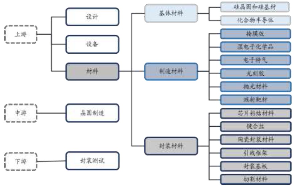
The semiconductor industry chain can be roughly divided into three main links: upstream links such as equipment, materials, and design, midstream wafer manufacturing, and downstream packaging and testing. Semiconductor materials are a very important link in the upstream link of the industry chain and play a key role in the production and manufacturing of chips. According to the semiconductor chip manufacturing process, semiconductor materials can generally be divided into three major materials: substrate, manufacturing, and packaging. Among them, substrate materials are mainly used to manufacture silicon wafer semiconductors or compound semiconductors. Manufacturing materials are mainly various materials required in the process of processing silicon wafers or compound semiconductors into chips. Packaging materials are materials used in the process of packaging and cutting the prepared chips.
Semiconductor materials are at the upstream of the entire industrial chain
Schematic diagram of semiconductor chip manufacturing process
Domestic enterprises are involved in the supply of materials in each link
1. Base material
According to the different chip materials, they are divided into silicon wafers and compound semiconductors. Among them, silicon wafers have the widest range of uses and are the most important raw materials in the manufacturing process of integrated circuits (ICs). All silicon wafers use single crystal silicon wafers, which have high requirements for the purity of silicon materials. Generally, the purity of silicon wafers is required to be above 99.9999999% (9N), which is much higher than the purity of photovoltaic-grade silicon wafers. First, single crystal silicon columns are prepared from silicon materials, and then single crystal silicon wafers are obtained after cutting. Generally, they can be divided into 6-18 inches according to different sizes. The current mainstream sizes are 8 inches (200mm) and 12 inches (300mm). 18 inches (450mm) is expected to gradually increase its market share at least after 2020. The global leading companies are mainly Shin-Etsu Chemical, SUMCO, GlobalWafers, Silitronic, LG and other companies.
Silicon wafer schematic
Compound semiconductors mainly refer to second- and third-generation semiconductors such as gallium arsenide (GaAs), gallium nitride (GaN) and silicon carbide (SiC). Compared with first-generation single-element semiconductors (such as semiconductors formed by silicon (Si) and germanium (Ge), they are much better in high-frequency performance and high-temperature performance. Among the three major compound semiconductor materials, GaAs accounts for the majority and is mainly used in the communications field, with a global market capacity of nearly US$10 billion; GaN has better high-power and high-frequency performance and is mainly used in the military field. The current market capacity is less than US$1 billion, and it is expected to be widely used as costs decrease; SiC is mainly used as a high-power semiconductor material, usually used in automobiles and industrial power electronics, and is widely used in the field of high-power conversion.
2. Manufacturing materials
Polishing materials
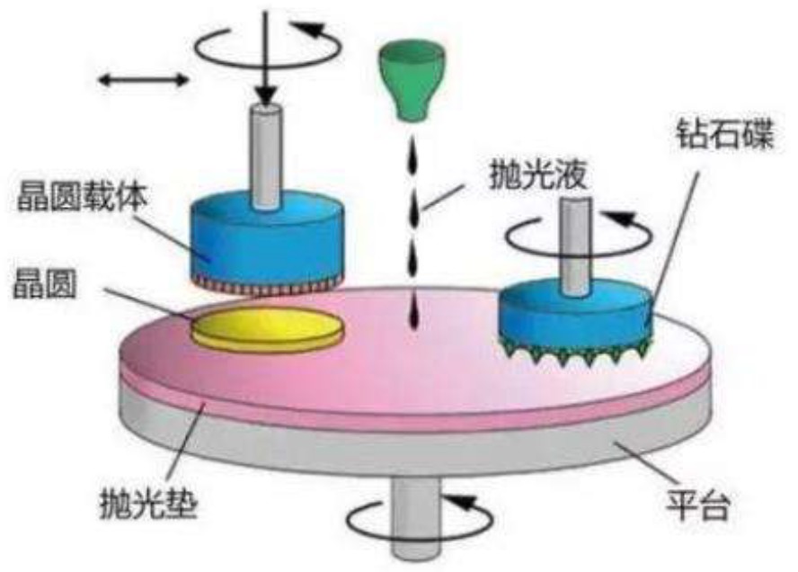
Polishing materials in semiconductors generally refer to materials used in the CMP (Chemical Mechanical Polishing) process. CMP polishing is a key process to achieve global uniform flatness of wafers. The principle of CMP polishing is that under a certain pressure and in the presence of polishing slurry, the workpiece being polished moves relative to the polishing pad, and a smooth surface is formed on the surface of the workpiece being polished by the organic combination of the grinding effect of nanoparticles and the corrosion effect of oxidants.
Schematic diagram of semiconductor polishing principle
Polishing materials can generally be divided into polishing pads, polishing liquids, conditioners and cleaners, of which the first two are the most critical. The material of the polishing pad is generally polyurethane or saturated polyurethane added to polyester, and the polishing liquid is generally composed of ultra-fine solid particle abrasives (such as nano-scale silica, aluminum oxide particles, etc.), surfactants, stabilizers, oxidants, etc.
According to data from SEMI and IC Mtia, the global polishing material market size was approximately US$1.61 billion in 2016, of which the domestic market size was approximately RMB 2.3 billion. The global polishing pad market is almost monopolized by Dow, while the polishing liquid market is mainly occupied by Fujimi and Hinomoto Kenmazai in Japan, Cabot, DuPont, Rodel, EKA in the United States, and ACE in South Korea.
Mask
The mask is also commonly known as a photomask, photomask, or photolithography mask. It is the carrier of the design pattern in the semiconductor chip photolithography process. Through photolithography and etching, the pattern is transferred to the silicon wafer. Masks usually choose different glass substrates according to different needs. Generally, quartz glass with low thermal expansion coefficient, low sodium content, high chemical stability, and high light transmittance is selected as the mainstream. An opaque chrome film with a thickness of about 100nm and chromium oxide with a thickness of about 20nm are plated on it to reduce light reflection.
According to data from SEMI and IC Mtia, the global semiconductor mask market size was approximately US$3.32 billion in 2018, of which the domestic market size was approximately RMB 5.95 billion. The global mask manufacturers are mainly Japan's TOPAN, Dai Nippon Printing, HOYA, SK Electronics, and the United States' Photronic.
Wet Electronic Chemicals
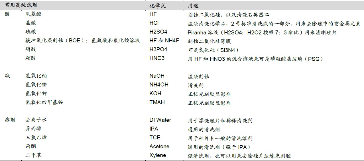
Wet electronic chemicals, also commonly known as ultra-clean high-purity reagents, refer to various high-purity chemical reagents used in the semiconductor manufacturing process. According to their uses, they can be divided into general chemicals and functional chemicals. General chemicals generally refer to high-purity pure chemical solvents, such as high-purity deionized water, hydrofluoric acid, sulfuric acid, phosphoric acid, nitric acid and other common reagents. In the process of manufacturing wafers, high-purity chemical solvents are mainly used to clean particles, organic residues, metal ions, natural oxide layers and other pollutants. Functional chemicals refer to formulated chemicals that achieve special functions through compounding and meet special process requirements in the manufacturing process, such as developers, stripping solutions, cleaning solutions, etching solutions, etc., which are often used in etching, sputtering and other process links.
High purity reagents commonly used in wet electronic chemicals
According to data from SEMI and IC Mtia, the global wet electronic chemicals market size was approximately US$1.11 billion in 2016, of which the domestic market size was approximately RMB 1.4 billion. The global market is mainly dominated by European, American and Japanese companies, including BASF and HenKel in Germany, Ashland, APM, Honeywell, ATMI, Airproducts in the United States, Sumitomo Chemical, Ube Industries, Wako Pure Chemical Industries, Nagase Industries, Mitsubishi Chemical and other companies in Japan.
Electronic special gas
Electronic special gases refer to various special gases that need to be used in the process of semiconductor chip preparation. According to the chemical composition of the gas, it can be divided into general gas and special gas. In addition, according to the purpose, it can also be divided into doping gas, epitaxy gas, ion implantation gas, light-emitting diode gas, etching gas, chemical vapor deposition gas and balance gas. Similar to high-purity reagents, electronic special gases also have extremely high requirements for gas purity, and basically require impurity content below ppt level. This is because the size of IC circuits has reached the nanometer level, and any trace amount of residual impurities in the gas may cause semiconductor short circuit or circuit damage.
Previous article:Pioneer develops next-generation 3D LiDAR sensor with a measurement distance of 500 meters
Next article:Tesla chips installed in over 600,000 vehicles reveal hidden features
- Popular Resources
- Popular amplifiers
- Car key in the left hand, liveness detection radar in the right hand, UWB is imperative for cars!
- After a decade of rapid development, domestic CIS has entered the market
- Aegis Dagger Battery + Thor EM-i Super Hybrid, Geely New Energy has thrown out two "king bombs"
- A brief discussion on functional safety - fault, error, and failure
- In the smart car 2.0 cycle, these core industry chains are facing major opportunities!
- The United States and Japan are developing new batteries. CATL faces challenges? How should China's new energy battery industry respond?
- Murata launches high-precision 6-axis inertial sensor for automobiles
- Ford patents pre-charge alarm to help save costs and respond to emergencies
- New real-time microcontroller system from Texas Instruments enables smarter processing in automotive and industrial applications
- Innolux's intelligent steer-by-wire solution makes cars smarter and safer
- 8051 MCU - Parity Check
- How to efficiently balance the sensitivity of tactile sensing interfaces
- What should I do if the servo motor shakes? What causes the servo motor to shake quickly?
- 【Brushless Motor】Analysis of three-phase BLDC motor and sharing of two popular development boards
- Midea Industrial Technology's subsidiaries Clou Electronics and Hekang New Energy jointly appeared at the Munich Battery Energy Storage Exhibition and Solar Energy Exhibition
- Guoxin Sichen | Application of ferroelectric memory PB85RS2MC in power battery management, with a capacity of 2M
- Analysis of common faults of frequency converter
- In a head-on competition with Qualcomm, what kind of cockpit products has Intel come up with?
- Dalian Rongke's all-vanadium liquid flow battery energy storage equipment industrialization project has entered the sprint stage before production
- Allegro MicroSystems Introduces Advanced Magnetic and Inductive Position Sensing Solutions at Electronica 2024
- Car key in the left hand, liveness detection radar in the right hand, UWB is imperative for cars!
- After a decade of rapid development, domestic CIS has entered the market
- Aegis Dagger Battery + Thor EM-i Super Hybrid, Geely New Energy has thrown out two "king bombs"
- A brief discussion on functional safety - fault, error, and failure
- In the smart car 2.0 cycle, these core industry chains are facing major opportunities!
- The United States and Japan are developing new batteries. CATL faces challenges? How should China's new energy battery industry respond?
- Murata launches high-precision 6-axis inertial sensor for automobiles
- Ford patents pre-charge alarm to help save costs and respond to emergencies
- New real-time microcontroller system from Texas Instruments enables smarter processing in automotive and industrial applications
- Techniques for PCB board array vias
- EEWORLD University ---- Razavi Analog Integrated Circuit Tutorial (English)
- How to interconnect DSP5509A and ARM
- 【Industrial Production Process PDA】Material Unboxing Post- DISCOVERY KIT WITH STM32F7508-DK
- Will 3D Touch be popular in the future?
- Car maintenance oscilloscope detection Volvo S80 fan does not rotate
- 2021 Electronics Contest E Question - Analog digital signal hybrid transmission transceiver, how to do it from scratch, is there any guiding post
- 【GD32E503 Review】One-month test summary
- 【Goodbye 2021, Hello 2022】I have become a father
- Big Baby Sleeping Assistant-Unfinished


 Chip Manufacturing: A Practical Tutorial on Semiconductor Process Technology (Sixth Edition)
 Designing Embedded Processors


 京公网安备 11010802033920号