Peripheral Interface (SPI) is one of the most widely used interfaces between microcontrollers and peripheral ICs (such as sensors, ADCs, DACs, shift registers, SRAM, etc.).
SPI is a synchronous, full-duplex, master-slave interface. Data from the master or slave is synchronized on the rising or falling edge of the clock. The master and slave can transmit data at the same time. The SPI interface can be 3-wire or 4-wire. This article focuses on the commonly used 4-wire SPI interface.
interface
4-wire SPI devices have four signals:
Clock (SPICLK,SCLK)
Chip select (CS) host output
Slave input (MOSI) master input
Slave output (MISO)
The device that generates the clock signal is called the host. Data transferred between the master and slave is synchronized with the clock generated by the master. Compared with the I2C interface, SPI devices support higher clock frequencies. Users should consult the product data sheet for clock frequency specifications of the SPI interface.
The SPI interface can only have one master, but can have one or more slaves. Figure 1 shows the SPI connection between the master and slave.
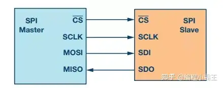
Figure 1. SPI configuration with master and slave
The chip select signal from the master is used to select the slave. This is usually an active low signal that disconnects the slave from the SPI bus when pulled high. When using multiple slaves, the master needs to provide a separate chip select signal for each slave. The chip select signal in this article is always an active low signal.
MOSI and MISO are data lines. MOSI sends data from the master to the slave, and MISO sends data from the slave to the master.
data transmission
To start SPI communication, the master must send a clock signal and select the slave by enabling the CS signal. Chip select is usually an active low signal. Therefore, the master must send a logic 0 on this signal to select the slave.
SPI is a full-duplex interface, and the host and slave can send data simultaneously through MOSI and MISO lines respectively. During SPI communication, the transmission of data (serial shifting out onto the MOSI/SDO bus) and reception (sampling or reading data on the bus (MISO/SDI)) occur simultaneously. The serial clock edge synchronizes the shifting and sampling of data.
The SPI interface allows the user the flexibility to select the rising or falling edge of the clock to sample and/or shift data. To determine the number of data bits transferred using the SPI interface, refer to the device data sheet.
Clock polarity and clock phase
In SPI, the host can select clock polarity and clock phase. During the idle state, the CPOL bit sets the polarity of the clock signal. The idle state refers to the period when CS is high level and transitioning to low level at the beginning of transmission, and the period when CS is low level and transitioning to high level at the end of transmission. The CPHA bit selects the clock phase.
Depending on the state of the CPHA bit, the rising or falling edge of the clock is used to sample and/or shift data. The master must select the clock polarity and clock phase based on the slave's requirements. There are four SPI modes available depending on the selection of CPOL and CPHA bits. Table 1 shows these 4 SPI modes.
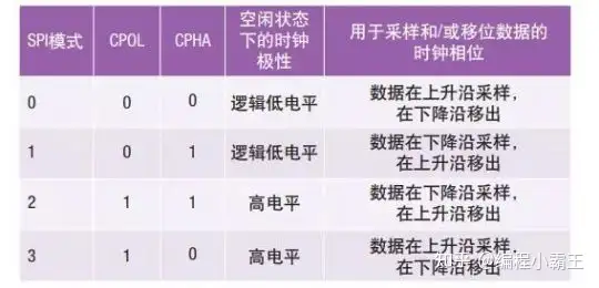
Table 1. SPI mode selection via CPOL and CPHA
Figures 2 to 5 show communication examples in the four SPI modes. In these examples, the data is shown on the MOSI and MISO lines. The start and end of the transfer are represented by green dashed lines, the sampling edges are represented by orange dashed lines, and the shift edges are represented by blue dashed lines. Please note that these graphics are for reference only. For successful SPI communication, the user must refer to the product data sheet and ensure that the device's timing specifications are met.
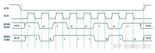
Figure 2. SPI Mode 0, CPOL = 0, CPHA = 0: CLK idle state = low, data is sampled on the rising edge and shifted out on the falling edge
Figure 3 shows the timing diagram for SPI Mode 1. In this mode, the clock polarity is 0, indicating that the idle state of the clock signal is low. The clock phase in this mode is 1, which means data is sampled on the falling edge (shown by the orange dashed line), and data is shifted out on the rising edge of the clock signal (shown by the blue dashed line).

Figure 3. SPI Mode 1, CPOL = 0, CPHA = 1: CLK idle state = low, data is sampled on the falling edge and shifted out on the rising edge

Figure 4. SPI Mode 2, CPOL = 1, CPHA = 1: CLK idle state = high, data is sampled on the falling edge and shifted out on the rising edge
Figure 4 shows the timing diagram for SPI Mode 2. In this mode, the clock polarity is 1, indicating that the idle state of the clock signal is high. The clock phase in this mode is 1, which means data is sampled on the falling edge (shown by the orange dashed line), and data is shifted out on the rising edge of the clock signal (shown by the blue dashed line).
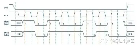
Figure 5. SPI Mode 3, CPOL = 1, CPHA = 0: CLK idle state = high, data is sampled on the rising edge and shifted out on the falling edge
Figure 5 shows the timing diagram for SPI Mode 3. In this mode, the clock polarity is 1, indicating that the idle state of the clock signal is high. The clock phase in this mode is 0, meaning data is sampled on the rising edge (shown by the orange dashed line), and data is shifted out on the falling edge of the clock signal (shown by the blue dashed line).
Multi-Slave Configuration
Multiple slaves can be used with a single SPI master. Slaves can be connected in regular mode or in daisy chain mode.
Regular SPI mode
In normal mode, the master needs to provide a separate chip select signal for each slave. Once the master enables (pulls low) the chip select signal, the clock and data on the MOSI/MISO lines are available to the selected slave. If multiple chip select signals are enabled, the data on the MISO line will be corrupted because the master cannot identify which slave is transmitting data.
As can be seen from Figure 6, as the number of slaves increases, the number of chip select lines from the host also increases. This quickly increases the number of inputs and outputs the master needs to provide and limits the number of slaves that can be used. Other techniques can be used to increase the number of slaves in normal mode, such as using multiplexers to generate chip select signals.
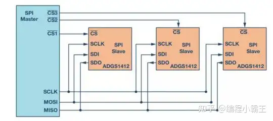
Figure 6. Multi-slave SPI configuration
Daisy chain mode
In daisy chain mode, the chip select signals of all slaves are connected together and data is propagated from one slave to the next. In this configuration, all slaves receive the same SPI clock at the same time. Data from the master goes directly to the first slave, which feeds the data to the next slave, and so on.
When using this method, since data is propagated from one slave to the next, the number of clock cycles required to transfer the data is proportional to the slave position in the daisy chain. For example, in the 8-bit system shown in Figure 7, in order for the third slave to obtain data, 24 clock pulses are required, while only 8 clock pulses are needed in conventional SPI mode.
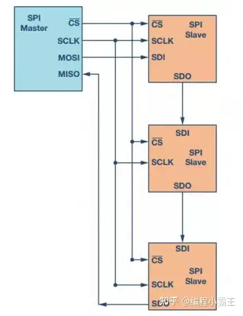
Figure 7. Multi-slave SPI daisy chain configuration
Figure 8 shows the clock cycles and data propagation through the daisy chain. Not all SPI devices support daisy chain mode. Please refer to the product datasheet to confirm if daisy chaining is available.
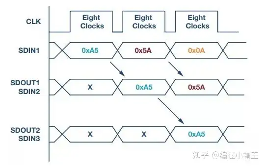
Figure 8. Daisy chain configuration: data dissemination
ADI SPI-enabled analog switches and multiplexers
Analog Devices' latest generation of SPI-enabled switches offers significant space savings without compromising precision switching performance. This section of the article discusses a case study illustrating how an SPI-enabled switch or multiplexer can greatly simplify system-level design and reduce the number of GPIOs required.
The ADG1412 is a quad-channel, single-pole single-throw (SPST) switch that requires four GPIOs connected to the control inputs of each switch. Figure 9 shows the connection between the microcontroller and an ADG1412.
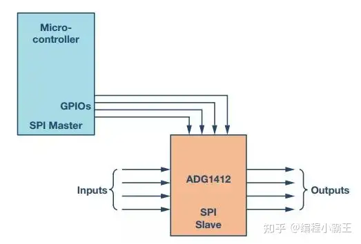
Figure 9. Microcontroller GPIO used as control signal for switch
As the number of switches on a circuit board increases, the number of required GPIOs increases significantly. For example, when designing a test instrumentation system, a large number of switches are used to increase the number of channels in the system. In a 4×4 crosspoint matrix configuration, four ADG1412s are used. This system requires 16 GPIOs, limiting the available GPIOs in standard microcontrollers. Figure 10 shows four ADG1412s connected using the microcontroller’s 16 GPIOs.
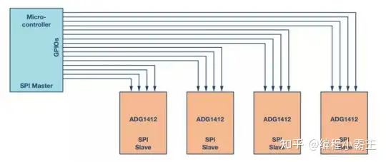
Figure 10. In a multi-slave configuration, the number of required GPIOs increases significantly
How to reduce the number of GPIOs?
One approach is to use a serial-to-parallel converter, as shown in Figure 11. The parallel signal output by the device can be connected to the switch control input, and the device can be configured through the serial interface SPI. The disadvantage of this method is that adding additional components will increase the bill of materials.
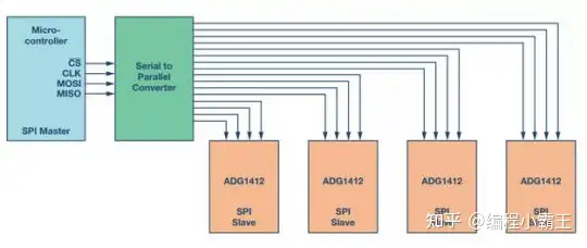
Figure 11. Multi-slave switch using serial-to-parallel converter
Another approach is to use an SPI controlled switch. The advantage of this approach is that it reduces the number of GPIOs required and also eliminates the overhead of an external serial-to-parallel converter. As shown in Figure 12, instead of 16 microcontroller GPIOs, only 7 microcontroller GPIOs are needed to provide SPI signals to 4 ADGS1412s. The switches can be configured in a daisy chain to further optimize GPIO count. In a daisy chain configuration, no matter how many switches the system uses, only the four GPIOs of the host (microcontroller) are used.
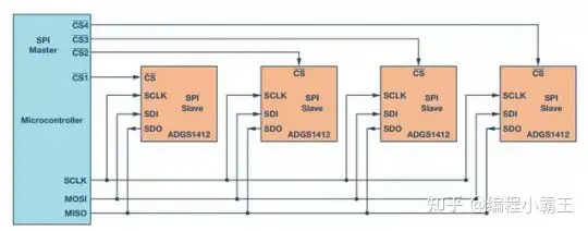
Figure 12. SPI-enabled switch saves microcontroller GPIO
Figure 13 is for illustration purposes. The ADGS1412 data sheet recommends using a pull-up resistor on the SDO pin. For simplicity, this example uses four switches. As the number of switches in a system increases, the advantages of circuit board simplicity and space savings are important.
Previous article:How should I learn microcontroller? Can it be done quickly?
Next article:Why do others learn microcontrollers so quickly?
- Popular Resources
- Popular amplifiers
 Professor at Beihang University, dedicated to promoting microcontrollers and embedded systems for over 20 years.
- Innolux's intelligent steer-by-wire solution makes cars smarter and safer
- 8051 MCU - Parity Check
- How to efficiently balance the sensitivity of tactile sensing interfaces
- What should I do if the servo motor shakes? What causes the servo motor to shake quickly?
- 【Brushless Motor】Analysis of three-phase BLDC motor and sharing of two popular development boards
- Midea Industrial Technology's subsidiaries Clou Electronics and Hekang New Energy jointly appeared at the Munich Battery Energy Storage Exhibition and Solar Energy Exhibition
- Guoxin Sichen | Application of ferroelectric memory PB85RS2MC in power battery management, with a capacity of 2M
- Analysis of common faults of frequency converter
- In a head-on competition with Qualcomm, what kind of cockpit products has Intel come up with?
- Dalian Rongke's all-vanadium liquid flow battery energy storage equipment industrialization project has entered the sprint stage before production
- Allegro MicroSystems Introduces Advanced Magnetic and Inductive Position Sensing Solutions at Electronica 2024
- Car key in the left hand, liveness detection radar in the right hand, UWB is imperative for cars!
- After a decade of rapid development, domestic CIS has entered the market
- Aegis Dagger Battery + Thor EM-i Super Hybrid, Geely New Energy has thrown out two "king bombs"
- A brief discussion on functional safety - fault, error, and failure
- In the smart car 2.0 cycle, these core industry chains are facing major opportunities!
- The United States and Japan are developing new batteries. CATL faces challenges? How should China's new energy battery industry respond?
- Murata launches high-precision 6-axis inertial sensor for automobiles
- Ford patents pre-charge alarm to help save costs and respond to emergencies
- New real-time microcontroller system from Texas Instruments enables smarter processing in automotive and industrial applications
- 100 ways to make power amplifiers
- User feedback post
- "Operational Amplifier Parameter Analysis and LTspice Application Simulation" Reading Notes: Chapter 1 Operational Amplifier Basics
- How UBOOT boots the Linux kernel and passes parameters to the kernel
- μC/OS embedded real-time operating system releases new open source version
- STEVAL-MKI109V3+ Test Basics
- Is there a “great theorist” around you?
- Built-in numeric keyboard to input numeric variable values
- Unboxing of Materials - STM32F7508 & ESP32
- Gigabit Network Contactless Connector-SK202 Evaluation 4: Strict Test Conditions, Reliable Test Data


 Digilent Vivado library
 AUTOSAR MCAL Principles and Practice
 Interactive Design between Arduino and LabVIEW


 京公网安备 11010802033920号