1 Introduction
Customers have reported that during the mass production phase, they found that the RTC of some products' MCUs did not work properly at low temperatures (0°C), but worked normally at room temperature. In addition, the RTC of other normal MCUs worked normally at both room and low temperatures.
2. Follow-up and analysis of issues
Through email communication with the customer, we learned that the MCU model used by the customer is: STM32F030C6T6TR. It is mainly used for power management and clock management in the master-slave structure of the product. According to the customer's description, it seems that different chips of the same model have large differences.
Due to time constraints, we visited the customer immediately after learning the preliminary information and conducted targeted tests on the MCU chip that the customer thought had problems. We generated a test project using STM32CubMx, using LSI (40K) and LSE (32.768K) respectively. When the RTC was working, the LED1 (PB5) was inverted once per second (whether the LED1 light flashed to indicate whether the RTC was working properly), and then measured the OSC pin and PA8 pin (output LSI or LSE) respectively, and compared them with the official ST NUCLEO-F030 board. The final test results are as follows:
| Test item | Temperature | Low-speed clock type | LED1(use PB5 to indicate the RTC status) | OSC pin | PA8 output clock |
|---|---|---|---|---|---|
| Use Customer board without any modify | Indoor temperature (25℃) | Use LSI(40KHz) | OK(Flash every second) | N/A | OK(Output 40K waveform) |
| Use Customer board without any modify | Under the low temperature(0℃) | Use LSI(40KHz) | OK(Flash every second) | N/A | OK(Output 40K waveform) |
| Use Customer board without any modify | Indoor temperature (25℃) | Use LSE(32.768KHz) | OK(Flash every second) | 32.768K waveform | OK(Output 32.768K waveform) |
| Use Customer board without any modify | Under the low temperature(0℃) | Use LSE(32.768KHz) | Failed(no flash) | 32.768K waveform detected | Failed(no output waveform) |
| Use the Customer board and modify the LSE load capacity value to 6.8pF | Indoor temperature (25℃) | Use LSE(32.768KHz) | OK(Flash every second) | 32.768K waveform | OK(Output 32.768K waveform) |
| Use the Customer board and modify the LSE load capacity value to 6.8pF | Under the low temperature(0℃) | Use LSE(32.768KHz) | OK(Flash every second) | 32.768K waveform | OK(Output 32.768K waveform) |
| Use ST Nucleo-F030 board | Indoor temperature (25℃) | Use LSE(32.768KHz) | OK(Flash every second) | 32.768K waveform | OK(Output 32.768K waveform) |
| Use ST Nucleo-F030 board | Under the low temperature(0℃) | Use LSE(32.768KHz) | OK(Flash every second) | 32.768K waveform | OK(Output 32.768K waveform) |
Through the test results, we get the following information:
When using LSI, it can work normally regardless of normal temperature or low temperature.
When using LSE, it can work normally at room temperature, but at low temperature (0℃), RTC no longer works (LED1 stops flashing), and the PA8 pin has no output, but remains at a high level, and at this time the OSC pin has a 32.768K waveform.
By changing the capacitance value of load capacitors C1 & C2 from 5.1pF to 6.8pF, the RTC that did not work at low temperature can resume normal operation.
Compared with ST's official NUCLEO-F030 board, it can work normally at both normal and low temperatures.
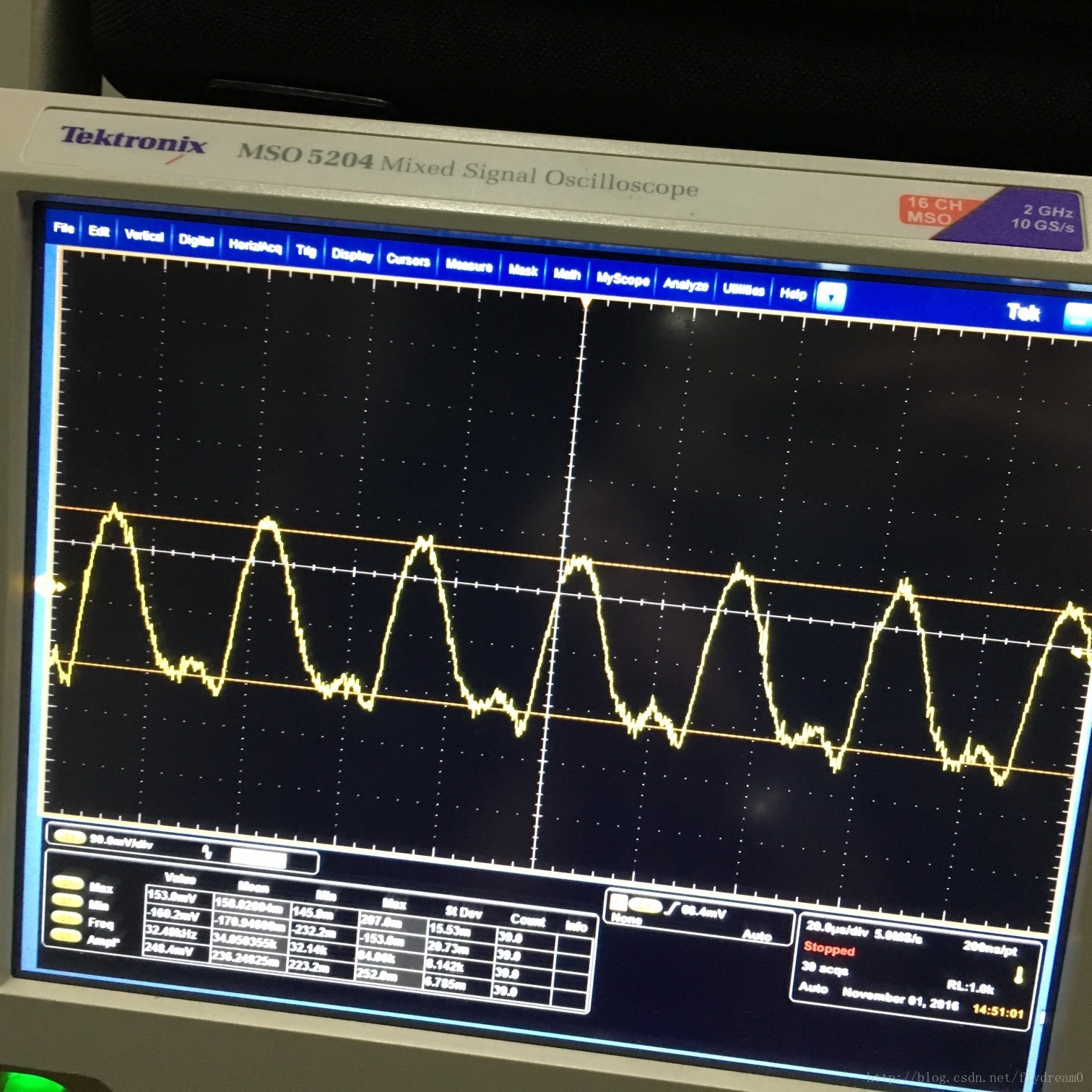
Figure 1 OSC foot waveform at low temperature 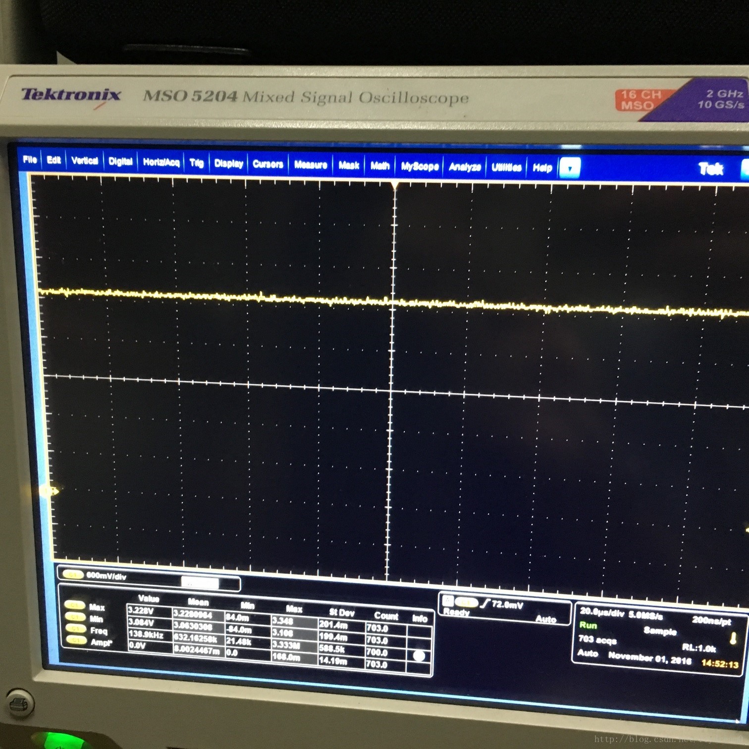
Figure 2 Waveform of PA8 pin at low temperature
From the test results, it can be seen that by modifying the load capacitance, the RTC that was not working properly can be restored to normal operation. This seems to be due to the fact that the customer's load capacitance cannot accurately match the system.
However, the customer did not accept this explanation, on the grounds that the current designed load capacitance of 5.1pF was a tested value with an accuracy of 6.5ppm. However, if it was changed to 6.8pF, the accuracy would be reduced to about 30ppm, which would seriously affect the time accuracy of the MCU's RTC. After the system had been running for a long time, the time would inevitably deviate greatly, exceeding the reasonable design range, which was not allowed.
3 Problem Analysis
Since the customer does not accept the modification of the load capacitance, we first review the various parameters of the customer's crystal oscillator design to see if they are accurate. The customer's LSE circuit design is shown below:

As shown in the figure above, the MR10 10Mohm feedback resistor is not added in the actual circuit. The crystal oscillator used is TXC. The relevant parameters obtained from the data sheet provided by the crystal oscillator manufacturer are as follows:
| index | parameters | Sym | Typical | Unit |
|---|---|---|---|---|
| 1 | Nominal Frequency | F0 | 32.768 | KHz |
| 2 | Load Capacitance | CL | 7.0 | pF |
| 3 | Equivalent Series Resistance | ESR | 70 | KΩ |
| 4 | Shunt Capacitance | C0 | 1.0 | pF |
Furthermore, since the LSE drive used in the customer code is configured at the highest level, the corresponding gm value can be found in the data sheet corresponding to the chip in the figure below, which is 25uA/V, and the drive current at this time is 1.6uA:

The above picture mentions the document AN2867, so we open this document and find this requirement in Section 3.4:

That is to say, the gain margin value is required to be greater than 5, so that the crystal oscillator can start normally. So how is the gain margin calculated? Next, find the calculation formula of gainmargin, as follows:

Among them, gm is the transconductance value mentioned in the data sheet in Figure 4. Different drive levels of STM32F030 LSE correspond to different gm values. Since our test code uses the code automatically generated by CubeMx, it uses the highest level by default, and the customer also uses the highest level. Therefore, the gm value obtained is 25 uA/V. With gm, how to calculate gmcrit in the above formula? Next, we find its calculation formula, such as:
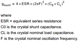
Through the corresponding parameters of the crystal oscillator, we can deduce:
ESR =70KΩ, C0 =1.0pF, CL =7.0pF, and F is the frequency of LSE, which is 32.768KHz.
So:
g_mcrit =4 * 7E4 * POWER(2*PI()32768,2) POWER ((1.0E-12 + 7.0E-12),2) =7.6E-07Finally
we get:
gain_magin =gm/g_mcrit =2.5E-05/7.6E-07 =32.89This
value is much larger than 5. Therefore, theoretically there is no problem of crystal oscillator not oscillating. In fact, when it is at low temperature, it was found in the previous test that the crystal oscillator also oscillates and has waveform output, but there is no waveform output at the PA8 pin. What is the problem?
Submitted to the division, and finally located that the LSE driver level was too high. In the document AN2867, there is such a description:

That is to say, in STM32F0 and STM32F3, when using the highest drive mode (gm_crit_max=5uA/V), it should only be used on a crystal with CL=12.5pF to avoid saturation of the oscillation loop, which can lead to startup failure. If a smaller CL (such as CL=6pF) is used at this time, the oscillation frequency will be unstable and the duty cycle may be distorted.
AN2867 then gives a table listing the relationship between the drive level and gm_min and gm_crit_max, as follows:

As shown above, for STM32F0, when using the highest drive mode High, gm_min = 25 uA/V, which is consistent with the data sheet. In addition, gm_crit_max = 5uA/V, which is exactly described above.
That is to say, in the highest drive mode, the corresponding CL should be 12.5pF, but the CL used by the customer is 7pF, which is inconsistent with the manual recommendations. As can be seen from Figure 4, in the highest drive level mode, the drive current is the largest (1.6uA), but a relatively small load capacitor (CL=7pF) is used here. According to AN2867, this may lead to saturation of the oscillation loop, unstable oscillation, and distorted duty cycle.
At this time, the LSE drive level should be lowered accordingly to reduce the drive current. If estimated proportionally here (12.5pF/1.6uA=7pF/xuA == > x=1.6*7/12.5 =0.89uA), except for the highest level, all others are acceptable. To be conservative, Medium High is relatively appropriate.
Open the reference manual of STM32F030, in section 7.4.9:
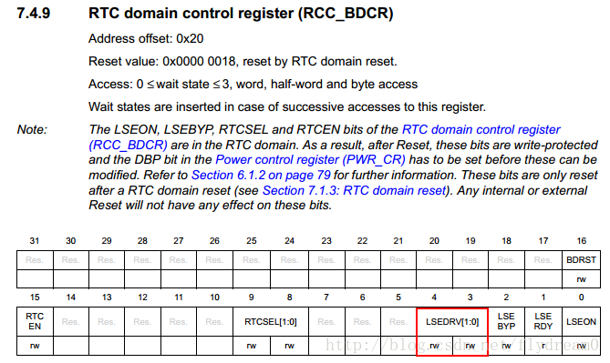
As shown in the figure above, just modify the two bits LSEDRV[1:0] to 10. After modifying the MCU chip that originally had RTC problems at low temperatures, it was put under low temperatures again for verification, and the test result was normal. Since this problem may occur in some chips, customers need to continue to track the modified chips. So far, there has been no feedback on this problem, so this problem is basically solved.
In addition, from the test results in Figure 1, in fact, under low temperature conditions, when the RTC has problems, the OSC pin can still capture the waveform normally, but there is no waveform on the MCO of the PA8 pin, which is just maintained at a high level. Therefore, for the saturation of the oscillation circuit caused by excessive driving current, unstable oscillation, and distorted working cycle, it is understood here that the connection point between the MCO pin and the internal oscillation circuit of the MCU is the waveform displayed by the MCO.
3 Conclusion
The document AN2867 summarizes information about STM32 crystal matching. It mentions that the larger the load capacitance CL value, the larger the required drive current, but the smaller the pull degree. This also explains the phenomenon in Table 1 that by increasing the capacitance value of C1&C2, the RTC that was originally problematic can be restored to normal. This is because the increase in the capacitance value of C1&C2 will cause the load capacitance CL to increase, and the corresponding required drive current will also increase, which in turn reduces the chance of saturation of the oscillation loop in the high drive mode.
In general, when it comes to crystal oscillators, we tend to focus on the calculation of gain margin. If its value is too small, it will lead to non-oscillation. But at the same time, we should also pay due attention to the situation where the oscillation loop is saturated due to excessive driving current.
The Chinese version of the document AN2867 is a simplified version. If you want to truly study it, it is recommended that you read the original English version.
Previous article:Startup assembly analysis of STM32F10x
Next article:The serial port sometimes receives abnormally when working in DMA mode
Recommended ReadingLatest update time:2024-11-16 16:42

- Popular Resources
- Popular amplifiers
 Professor at Beihang University, dedicated to promoting microcontrollers and embedded systems for over 20 years.
- Innolux's intelligent steer-by-wire solution makes cars smarter and safer
- 8051 MCU - Parity Check
- How to efficiently balance the sensitivity of tactile sensing interfaces
- What should I do if the servo motor shakes? What causes the servo motor to shake quickly?
- 【Brushless Motor】Analysis of three-phase BLDC motor and sharing of two popular development boards
- Midea Industrial Technology's subsidiaries Clou Electronics and Hekang New Energy jointly appeared at the Munich Battery Energy Storage Exhibition and Solar Energy Exhibition
- Guoxin Sichen | Application of ferroelectric memory PB85RS2MC in power battery management, with a capacity of 2M
- Analysis of common faults of frequency converter
- In a head-on competition with Qualcomm, what kind of cockpit products has Intel come up with?
- Dalian Rongke's all-vanadium liquid flow battery energy storage equipment industrialization project has entered the sprint stage before production
- Allegro MicroSystems Introduces Advanced Magnetic and Inductive Position Sensing Solutions at Electronica 2024
- Car key in the left hand, liveness detection radar in the right hand, UWB is imperative for cars!
- After a decade of rapid development, domestic CIS has entered the market
- Aegis Dagger Battery + Thor EM-i Super Hybrid, Geely New Energy has thrown out two "king bombs"
- A brief discussion on functional safety - fault, error, and failure
- In the smart car 2.0 cycle, these core industry chains are facing major opportunities!
- The United States and Japan are developing new batteries. CATL faces challenges? How should China's new energy battery industry respond?
- Murata launches high-precision 6-axis inertial sensor for automobiles
- Ford patents pre-charge alarm to help save costs and respond to emergencies
- New real-time microcontroller system from Texas Instruments enables smarter processing in automotive and industrial applications
- Watch the keynote speech by Rohde & Schwarz to get a more intuitive understanding of 5G. Fill out the questionnaire to win prizes!
- Taking over low-speed parking tasks – 360-degree surround view and automatic parking system
- [AB32VG1 Development Board Review] Dual Serial Port Communication and Problems
- Share the method of safely measuring 220V mains electricity with an oscilloscope
- When the STM32F407 PWM is outputting, one interrupt is not completed and the next interrupt is entered, resulting in a disordered output waveform
- 【Example】Wireless serial port module star network networking case
- 【GD32F310G-START Review】Review 2: GD32F301 driving Nokia 5110LCD
- Studying Things to Gain Knowledge 03: In DC circuits, energy is not transmitted by wires either
- [TI recommended course] #TI's new generation C2000? microcontroller: full support for servo and motor drive applications#
- Does anyone have a PDF of Analog Filter and Circuit Design Handbook (US)?


 Automotive Electronics S32K Series Microcontrollers: Based on ARM Cortex-M4F Core
 Conquering video technology


 京公网安备 11010802033920号