1. Basic knowledge
ADC0809 is a CMOS component with an 8-bit A/D converter, an 8-way multiplexer, and microprocessor-compatible control logic. It is a successive approximation A/D converter that can be directly interfaced with a single-chip microcomputer.
(1) Internal logic structure of ADC0809
8-way analog switch
8-way A/D converter
Three-state output latch
Address latch and decoder
IN0
IN1
IN2
IN3
IN4
IN5
IN6
IN7
A
B
C
ALE
VREF(+)
VREF(-)
OE
EOC
D0
D1
D2
D3
D4
D5
D6
D7
CLK
ST


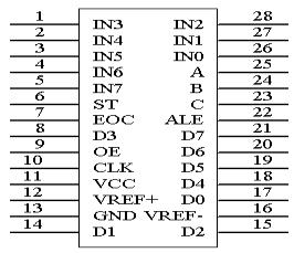
As can be seen from the figure above, ADC0809 consists of an 8-way analog switch, an address latch and decoder, an A/D converter, and a three-state output latch. The multiplexer can select 8 analog channels, allowing 8 analog inputs to be time-sharing and converted using the shared A/D converter. The three-state output latch is used to latch the digital quantity after A/D conversion. When the OE terminal is at a high level, the converted data can be taken from the three-state output latch.
(2)
Pin structure
IN0-IN7: 8 analog input channels
ADC0809 has the following requirements for input analog quantity: the signal is unipolar, the voltage range is 0-5V, if the signal is too small, it must be amplified; the input analog quantity should remain unchanged during the conversion process. If the analog quantity changes too quickly, a sampling and holding circuit must be added before the input.
Address input and control lines: 4
ALE are address latch enable input lines, and high level is valid. When the ALE line is at a high level, the address latch and decoder latch the address signals of the three address lines A, B, and C. After decoding, the analog quantity of the selected channel enters the converter for conversion. A, B, and C are address input lines, which are used to select one analog input on IN0-IN7. The channel selection table is shown in the following table.
C
B
A
Selected channel
0
0
0
IN0
0
0
1
IN1
0
1
0
IN2
0
1
1
IN3 1 0 0 IN4
1
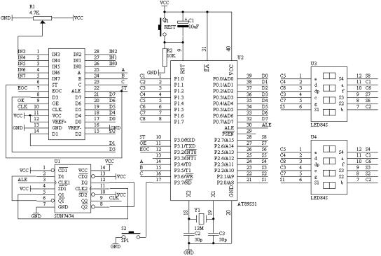
0 1 IN5 1 1 0 IN6 1 1 1 IN7 Digital output and control lines: 11 lines ST is the conversion start signal. When ST jumps up, all internal registers are cleared; when it jumps down , A/D conversion begins; during the conversion, ST should remain low. EOC is the conversion end signal. When EOC is high, it indicates that the conversion is over; otherwise, it indicates that A/D conversion is in progress. OE is the output enable signal, which is used to control the three output latches to output the converted data to the microcontroller. OE=1, output the converted data; OE=0, the output data line is in high impedance state. D7-D0 are digital output lines. CLK is the clock input signal line. Since there is no clock circuit inside ADC0809, the required clock signal must be provided by the outside world. The frequency used is usually 500KHZ. VREF (+) and VREF (-) are reference voltage inputs. 2. ADC0809 Application Notes (1) ADC0809 has an internal output latch and can be directly connected to the AT89S51 microcontroller. (2) During initialization, make the ST and OE signals all low. (3) Send the address of the channel to be converted to the A, B, and C ports. (4) Give a positive pulse signal with a width of at least 100ns at the ST terminal. (5) Whether the conversion is completed, we judge based on the EOC signal. (6) When EOC becomes high, OE is high at this time, and the converted data is output to the microcontroller. 3. The experimental task is as shown in the figure below. Input an analog quantity between 0 and 5V from the channel IN3 of ADC0809, which is converted into a digital quantity by ADC0809 and displayed in decimal on the digital tube. VREF of ADC0809 is connected to +5V voltage. 4. Circuit Schematic Diagram

Figure 1.27.1
5. Hardware connection on the system board
(1). Connect P1.0-P1.7 of the P1 port in the "MCU system board" area to the A B C D E F G H port in the "Dynamic digital display" area with an 8-core cable, as the pen segment driver of the digital tube.
(2). Connect P2.0-P2.7 of the P2 port in the "MCU system board" area to the S1 S2 S3 S4 S5 S6 S7 S8 port in the "Dynamic digital display" area with an 8-core cable, as the bit segment selection of the digital tube.
(3). Connect P0.0-P0.7 of the P0 port in the "MCU system board" area to the D0 D1 D2 D3 D4 D5 D6 D7 port in the "Analog-to-digital conversion module" area with an 8-core cable, and the A/D converted data is input to the P0 port of the MCU
(4). Connect the VREF terminal in the "Analog-to-Digital Conversion Module" area to the VCC terminal in the "Power Supply Module" area with a wire.
(5) Connect the A2A1A0 terminal in the "Analog-to-Digital Conversion Module" area to the P3.4 P3.5 P3.6 terminal in the "Microcontroller System" area with a wire.
(6) Connect the ST terminal in the "Analog-to-Digital Conversion Module" area to the P3.0 terminal in the "Microcontroller System" area with a wire.
(7) Connect the OE terminal in the "Analog-to-Digital Conversion Module" area to the P3.1 terminal in the "Microcontroller System" area with a wire.
(8) Connect the EOC terminal in the "Analog-to-Digital Conversion Module" area to the P3.2 terminal in the "Microcontroller System" area with a wire.
(9) Connect the CLK terminal in the "Analog-to-Digital Conversion Module" area to the /4 terminal in the "Frequency Divider Module" area with a wire.
(10) Connect the CK IN terminal in the "frequency division module" area to the ALE terminal in the "single chip system" area with a wire;
(11) Connect the IN3 terminal in the "analog-to-digital conversion module" area to the VR1 terminal in the "three-way adjustable voltage module" area with a wire;
6. Program design content
(1) When performing A/D conversion, use the EOC flag signal to detect whether the A/D conversion is completed. If it is completed, read the data through the P0 port and display it on the digital tube after data processing.
(2) Before performing A/D conversion, the method to start the conversion is:
ABC=110 select the third channel
ST=0, ST=1, ST=0 generate a positive pulse signal to start the conversion
7. Assembly source program
CH EQU 30H
DPCNT EQU 31H
DPBUF EQU 33H
GDATA EQU 32H
ST BIT P3.0
OE BIT P3.1
EOC BIT P3.2
ORG 00H
LJMP START
ORG 0BH
LJMP T0X
ORG 30H
START: MOV CH,#0BCH
MOV DPCNT,#00H
MOV R1,# DPCNT
MOV R7,#5
MOV A,#10
MOV R0,#DPBUF
LOP: MOV @R0,A
INC R0
DJNZ R7,LOP
MOV @R0,#00H
INC R0
MOV @R0,#00H
INC R0
MOV @R0,#00H
MOV TMOD,#01H
MOV TH0,#(65536-4000)/256
MOV TL0,#(65536-4000) MOD 256
SETB TR0
SETB ET0
SETB EA
WT: CLR ST
SETB ST
CLR ST
WAIT: JNB EOC,WAIT
SETB OE
MOV GDATA,P0
CLR OE
MOV A,GDATA
MOV B,#100
DIV AB
MOV 33H,A
MOV A,B
MOV B,#10
DIV AB
MOV 34H,A
MOV 35H,B
SJMP WT
T0X: NOP
MOV TH0,#(65536-4000)/256
MOV TL0,#(65536-4000) MOD 256
MOV DPTR,#DPCD
MOV A, DPCNT
ADD A,#DPBUF
MOV R0,A
MOV A,@R0
MOVC A,@A+DPTR
MOV P1,A
MOV DPTR,#DPBT
MOV A,DPCNT
MOVC A,@A+DPTR
MOV P2,A
INC DPCNT
MOV A ,DPCNT
CJNE A,#8,NEXT
MOV DPCNT,#00H
NEXT: RETI
DPCD: DB 3FH,06H,5BH,4FH,66H
DB 6DH,7DH,07H,7FH,6FH,00H
DPBT: DB 0FEH,0FDH,0FBH,0F7H
DB 0EFH,0DFH,0BFH,07FH
END
8. C language source program
#include
unsigned char code dispbitcode[]={0xfe,0xfd,0xfb,0xf7,
0xef,0xdf,0xbf,0x7f};
unsigned char code dispcode[]={0x3f,0x06,0x5b, 0x4f,0x66,
0x6d,0x7d,0x07,0x7f,0x6f,0x00};
unsigned char dispbuf[8]={10,10,10,10,10,0,0,0};
unsigned char dispcount;
sbit ST=P3 ^0;
sbit OE=P3^1;
sbit EOC=P3^2;
unsigned char channel=0xbc;//IN3
unsigned char getdata;
void main(void)
{
TMOD=0x01;
TH0=(65536-4000)/256;
TL0=(65536-4000)%256;
TR0=1;
ET0=1;
EA=1;
P3=channel;
while(1)
{
ST=0;
ST=1;
ST=0;
while(EOC==0);
OE=1;
getdata=P0;
OE=0;
dispbuf[2]=getdata/100;
getdata=getdata%10;
dispbuf[1 ]=getdata/10;
dispbuf[0]=getdata%10;
}
}
void t0(void) interrupt 1 using 0
{
TH0=(65536-4000)/256;
TL0=(65536-4000)%256;
P1=dispcode[dispbuf[dispcount]];
P2=dispbitcode[dispcount];
dispcount++;
if(dispcount==8)
{
dispcount=0;
}
}
Keywords:ADC0809
Reference address:27. Basic application technology of ADC0809 A/D converter
ADC0809 is a CMOS component with an 8-bit A/D converter, an 8-way multiplexer, and microprocessor-compatible control logic. It is a successive approximation A/D converter that can be directly interfaced with a single-chip microcomputer.
(1) Internal logic structure of ADC0809
8-way analog switch
8-way A/D converter
Three-state output latch
Address latch and decoder
IN0
IN1
IN2
IN3
IN4
IN5
IN6
IN7
A
B
C
ALE
VREF(+)
VREF(-)
OE
EOC
D0
D1
D2
D3
D4
D5
D6
D7
CLK
ST


(2)

IN0-IN7: 8 analog input channels
ADC0809 has the following requirements for input analog quantity: the signal is unipolar, the voltage range is 0-5V, if the signal is too small, it must be amplified; the input analog quantity should remain unchanged during the conversion process. If the analog quantity changes too quickly, a sampling and holding circuit must be added before the input.
Address input and control lines: 4
ALE are address latch enable input lines, and high level is valid. When the ALE line is at a high level, the address latch and decoder latch the address signals of the three address lines A, B, and C. After decoding, the analog quantity of the selected channel enters the converter for conversion. A, B, and C are address input lines, which are used to select one analog input on IN0-IN7. The channel selection table is shown in the following table.
C
B
A
Selected channel
0
0
0
IN0
0
0
1
IN1
0
1
0
IN2
0
1
1
IN3 1 0 0 IN4
1
0 1 IN5 1 1 0 IN6 1 1 1 IN7 Digital output and control lines: 11 lines ST is the conversion start signal. When ST jumps up, all internal registers are cleared; when it jumps down , A/D conversion begins; during the conversion, ST should remain low. EOC is the conversion end signal. When EOC is high, it indicates that the conversion is over; otherwise, it indicates that A/D conversion is in progress. OE is the output enable signal, which is used to control the three output latches to output the converted data to the microcontroller. OE=1, output the converted data; OE=0, the output data line is in high impedance state. D7-D0 are digital output lines. CLK is the clock input signal line. Since there is no clock circuit inside ADC0809, the required clock signal must be provided by the outside world. The frequency used is usually 500KHZ. VREF (+) and VREF (-) are reference voltage inputs. 2. ADC0809 Application Notes (1) ADC0809 has an internal output latch and can be directly connected to the AT89S51 microcontroller. (2) During initialization, make the ST and OE signals all low. (3) Send the address of the channel to be converted to the A, B, and C ports. (4) Give a positive pulse signal with a width of at least 100ns at the ST terminal. (5) Whether the conversion is completed, we judge based on the EOC signal. (6) When EOC becomes high, OE is high at this time, and the converted data is output to the microcontroller. 3. The experimental task is as shown in the figure below. Input an analog quantity between 0 and 5V from the channel IN3 of ADC0809, which is converted into a digital quantity by ADC0809 and displayed in decimal on the digital tube. VREF of ADC0809 is connected to +5V voltage. 4. Circuit Schematic Diagram

(1). Connect P1.0-P1.7 of the P1 port in the "MCU system board" area to the A B C D E F G H port in the "Dynamic digital display" area with an 8-core cable, as the pen segment driver of the digital tube.
(2). Connect P2.0-P2.7 of the P2 port in the "MCU system board" area to the S1 S2 S3 S4 S5 S6 S7 S8 port in the "Dynamic digital display" area with an 8-core cable, as the bit segment selection of the digital tube.
(3). Connect P0.0-P0.7 of the P0 port in the "MCU system board" area to the D0 D1 D2 D3 D4 D5 D6 D7 port in the "Analog-to-digital conversion module" area with an 8-core cable, and the A/D converted data is input to the P0 port of the MCU
(4). Connect the VREF terminal in the "Analog-to-Digital Conversion Module" area to the VCC terminal in the "Power Supply Module" area with a wire.
(5) Connect the A2A1A0 terminal in the "Analog-to-Digital Conversion Module" area to the P3.4 P3.5 P3.6 terminal in the "Microcontroller System" area with a wire.
(6) Connect the ST terminal in the "Analog-to-Digital Conversion Module" area to the P3.0 terminal in the "Microcontroller System" area with a wire.
(7) Connect the OE terminal in the "Analog-to-Digital Conversion Module" area to the P3.1 terminal in the "Microcontroller System" area with a wire.
(8) Connect the EOC terminal in the "Analog-to-Digital Conversion Module" area to the P3.2 terminal in the "Microcontroller System" area with a wire.
(9) Connect the CLK terminal in the "Analog-to-Digital Conversion Module" area to the /4 terminal in the "Frequency Divider Module" area with a wire.
(10) Connect the CK IN terminal in the "frequency division module" area to the ALE terminal in the "single chip system" area with a wire;
(11) Connect the IN3 terminal in the "analog-to-digital conversion module" area to the VR1 terminal in the "three-way adjustable voltage module" area with a wire;
6. Program design content
(1) When performing A/D conversion, use the EOC flag signal to detect whether the A/D conversion is completed. If it is completed, read the data through the P0 port and display it on the digital tube after data processing.
(2) Before performing A/D conversion, the method to start the conversion is:
ABC=110 select the third channel
ST=0, ST=1, ST=0 generate a positive pulse signal to start the conversion
7. Assembly source program
CH EQU 30H
DPCNT EQU 31H
DPBUF EQU 33H
GDATA EQU 32H
ST BIT P3.0
OE BIT P3.1
EOC BIT P3.2
ORG 00H
LJMP START
ORG 0BH
LJMP T0X
ORG 30H
START: MOV CH,#0BCH
MOV DPCNT,#00H
MOV R1,# DPCNT
MOV R7,#5
MOV A,#10
MOV R0,#DPBUF
LOP: MOV @R0,A
INC R0
DJNZ R7,LOP
MOV @R0,#00H
INC R0
MOV @R0,#00H
INC R0
MOV @R0,#00H
MOV TMOD,#01H
MOV TH0,#(65536-4000)/256
MOV TL0,#(65536-4000) MOD 256
SETB TR0
SETB ET0
SETB EA
WT: CLR ST
SETB ST
CLR ST
WAIT: JNB EOC,WAIT
SETB OE
MOV GDATA,P0
CLR OE
MOV A,GDATA
MOV B,#100
DIV AB
MOV 33H,A
MOV A,B
MOV B,#10
DIV AB
MOV 34H,A
MOV 35H,B
SJMP WT
T0X: NOP
MOV TH0,#(65536-4000)/256
MOV TL0,#(65536-4000) MOD 256
MOV DPTR,#DPCD
MOV A, DPCNT
ADD A,#DPBUF
MOV R0,A
MOV A,@R0
MOVC A,@A+DPTR
MOV P1,A
MOV DPTR,#DPBT
MOV A,DPCNT
MOVC A,@A+DPTR
MOV P2,A
INC DPCNT
MOV A ,DPCNT
CJNE A,#8,NEXT
MOV DPCNT,#00H
NEXT: RETI
DPCD: DB 3FH,06H,5BH,4FH,66H
DB 6DH,7DH,07H,7FH,6FH,00H
DPBT: DB 0FEH,0FDH,0FBH,0F7H
DB 0EFH,0DFH,0BFH,07FH
END
8. C language source program
#include
unsigned char code dispbitcode[]={0xfe,0xfd,0xfb,0xf7,
0xef,0xdf,0xbf,0x7f};
unsigned char code dispcode[]={0x3f,0x06,0x5b, 0x4f,0x66,
0x6d,0x7d,0x07,0x7f,0x6f,0x00};
unsigned char dispbuf[8]={10,10,10,10,10,0,0,0};
unsigned char dispcount;
sbit ST=P3 ^0;
sbit OE=P3^1;
sbit EOC=P3^2;
unsigned char channel=0xbc;//IN3
unsigned char getdata;
void main(void)
{
TMOD=0x01;
TH0=(65536-4000)/256;
TL0=(65536-4000)%256;
TR0=1;
ET0=1;
EA=1;
P3=channel;
while(1)
{
ST=0;
ST=1;
ST=0;
while(EOC==0);
OE=1;
getdata=P0;
OE=0;
dispbuf[2]=getdata/100;
getdata=getdata%10;
dispbuf[1 ]=getdata/10;
dispbuf[0]=getdata%10;
}
}
void t0(void) interrupt 1 using 0
{
TH0=(65536-4000)/256;
TL0=(65536-4000)%256;
P1=dispcode[dispbuf[dispcount]];
P2=dispbitcode[dispcount];
dispcount++;
if(dispcount==8)
{
dispcount=0;
}
}
Previous article:28. Digital voltmeter
Next article:51 MCU interrupt entry address representation in C language
Recommended ReadingLatest update time:2024-11-16 15:02
Keysight spectrum analyzer maintenance case--N9030A startup error repair

1. Fault phenomenon: 10db and above attenuation power is inaccurate; startup error Error finding operating system, operating system not found 2. Testing process After receiving the instrument, we first checked whether the instrument had passed the original factory warranty. After checking, the instrument had passed
[Test Measurement]

The function of startup.a51 program module of 80C51 microcontroller
The first program module executed by 80C51 after power on reset is not the user's main program main(), but a program module called startup.a51 hidden in the KEIL-C51 standard link library. . The main job of startup.a51 is to clear the memory blocks including idata, xdata, and pdata to 0 and initialize the recursive
[Microcontroller]
Samsung s5pv210 boot process (ARM Cortex-A8)
S5PV210 has 96Kb IRAM and 64Kb IROM. DRAM0 address: 0x2000_0000——0x3FFF_FFFF(512MB) (built-in memory) DRAM1 address: 0x4000_0000——0x7FFF_FFFF(1024MB) (extended memory) SROM address: 0x8000_0000——0xAFFF_FFFF(128MB*6)(extended memory) IROM address: 0xD000_0000——0xD000_FFFF(64Kb) ISRAM address: 0xD002_0000——0xD003_7FFF(
[Microcontroller]
PIC16F877A - Timer 0
/****************************************************** *******
PIC16F877A_Timer0_Timer
*************************************************** ******/
#include "pic.h"
__CONFIG(0x3F71);
/****************************************************** *******
Timer 0 initialization function
************************
[Microcontroller]
Sony Xperia 1 II pushes Android 11 update, version 58.1.A.0.921
Sony officially released the Android 11 update for Xperia 1 II (XQ-AT52) today, with version number 58.1.A.0.921. Xperia 1 II in the Taiwan market has been the first to receive the update. IT Home has reported that Sony has announced the Android 11 update time for eligible Xperia phones. Xperia 5 II and Xperia
[Mobile phone portable]
Guangdong Xin's 12-inch wafer project went into production, and Zhiguang Electric became the big winner in the A-share market
On the evening of September 22, Zhiguang Electric issued an announcement stating that the company invested in and subscribed to 30% of the limited partner shares of Guangzhou Yuxin Zhongcheng Equity Investment Partnership (Limited Partnership) (hereinafter referred to as "Yuxin Zhongcheng"). Yuxin Zhongcheng holds 50%
[Mobile phone portable]
HT48R50A 4X4 button display program

; ******************************************** ; Function: 4X4 button, digital tube display program * ; MICroProcessor : HT48R50A-1/28SKDIP-A * ; Author: www.picavr.com * ; Crystal : 4MHz * ; ******************************************** #INCLUDE HT48
[Microcontroller]

Get μA level tiny constant current circuit diagram

Get μA level tiny constant current circuit diagram
[Power Management]

- Popular Resources
- Popular amplifiers
-
 Microgrid Stability Analysis and Control Microgrid Modeling Stability Analysis and Control to Improve Power Distribution and Power Flow Control (
 -
 Signal and System Experiment Tutorial (Edited by Jin Bo)
 -
 Effective Unit Testing (Lasse Koskela)
 -
 Operational Amplifier Practical Reference Handbook (Edited by Liu Changsheng, Zhao Mingying, Liu Xu, etc.)
Recommended Content
Latest Microcontroller Articles
He Limin Column
Microcontroller and Embedded Systems Bible
 Professor at Beihang University, dedicated to promoting microcontrollers and embedded systems for over 20 years.
MoreSelected Circuit Diagrams
MorePopular Articles
- Innolux's intelligent steer-by-wire solution makes cars smarter and safer
- 8051 MCU - Parity Check
- How to efficiently balance the sensitivity of tactile sensing interfaces
- What should I do if the servo motor shakes? What causes the servo motor to shake quickly?
- 【Brushless Motor】Analysis of three-phase BLDC motor and sharing of two popular development boards
- Midea Industrial Technology's subsidiaries Clou Electronics and Hekang New Energy jointly appeared at the Munich Battery Energy Storage Exhibition and Solar Energy Exhibition
- Guoxin Sichen | Application of ferroelectric memory PB85RS2MC in power battery management, with a capacity of 2M
- Analysis of common faults of frequency converter
- In a head-on competition with Qualcomm, what kind of cockpit products has Intel come up with?
- Dalian Rongke's all-vanadium liquid flow battery energy storage equipment industrialization project has entered the sprint stage before production
MoreDaily News
- Allegro MicroSystems Introduces Advanced Magnetic and Inductive Position Sensing Solutions at Electronica 2024
- Car key in the left hand, liveness detection radar in the right hand, UWB is imperative for cars!
- After a decade of rapid development, domestic CIS has entered the market
- Aegis Dagger Battery + Thor EM-i Super Hybrid, Geely New Energy has thrown out two "king bombs"
- A brief discussion on functional safety - fault, error, and failure
- In the smart car 2.0 cycle, these core industry chains are facing major opportunities!
- The United States and Japan are developing new batteries. CATL faces challenges? How should China's new energy battery industry respond?
- Murata launches high-precision 6-axis inertial sensor for automobiles
- Ford patents pre-charge alarm to help save costs and respond to emergencies
- New real-time microcontroller system from Texas Instruments enables smarter processing in automotive and industrial applications
Guess you like
- Dismantling and Renovation of Old LED Bulbs
- Emitter follower principle and typical circuit
- STM32 A certain function is put into RAM and runs without any phenomenon
- I searched Baidu for half an hour but couldn't find the answer. I used a search engine to find the answer in seconds.
- EEWORLD University Hall ---- Disassembling the front controller module of Tesla Model 3 VCFRONT
- How to use JTAG to program UCD90120A
- Creating a Superior Smart Display Experience with DLP Pico Technology
- Previous test questions of the measurement and control category of the electric competition
- instaSPIN-FOC Motor Starting
- TGF4042 Function Signal Generator Evaluation: Pulse Waveform Generation

 Microgrid Stability Analysis and Control Microgrid Modeling Stability Analysis and Control to Improve Power Distribution and Power Flow Control (


 京公网安备 11010802033920号