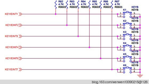
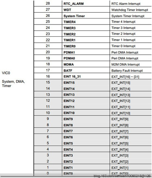
Outer board schematic

Four-layer board schematic diagram (core board)

This board uses a total of 10 keys, namely EINT1~EINT7
So the corresponding registers are GPH1_1~GPH0_7..
First, check the chip manual to see the descriptor of the GPH0 register.
GPH0,1,2,3: 32 in/out pin –CAM IF channel, Key pad, External Wakeup (up-to 32-bit)
The main idea is that GPHO can be woken up externally.
GPH0CON[7] [31:28] 0000 = Input, 0001 = Output, 0010 = WU_INT[7] 0000
GPH0CON[6] [27:24] 0000 = Input, 0001 = Output, 0010 = WU_INT[6] 0000
GPH0CON[5] [23:20] 0000 = Input, 0001 = Output, 0010 = WU_INT[5] 0000
GPH0CON[4] [19:16] 0000 = Input, 0001 = Output, 0010 = WU_INT[4] 0000
GPH0CON[3] [15:12] 0000 = Input, 0001 = Output, 0010 = WU_INT[3] 0000
GPH0CON[2] [11:8] 0000 = Input, 0001 = Output, 0010 = WU_INT[2] 0000
GPH0CON[1] [7:4] 0000 = Input, 0001 = Output, 0010 = WU_INT[1] 0000
PAD CONTROL S5PC100 USER’S MANUAL (REV1.0)
2.2-36
GPH0CON[0] [3:0] 0000 = Input, 0001 = Output, 0010 = WU_INT[0] 0000
Then let's look at the wake-up interrupt configuration register:
5.6.1 Wakeup Interrupt 0_7 Configuration (WU_INT0_7_CON, R/W, Address = 0xE030_0E00)
The value of WU_INTx_y_CON[n] means that 000 = Low level, 001 = High level, 010 = Falling edge triggered,
011 = Rising edge triggered, 100 = Both edge triggered
It means wake-up interrupt configuration register
000 is low level valid 001 is high level valid 010 is falling edge trigger 011 is rising edge trigger valid 100 is both edges are acceptable
Let's take a look at the wake-up interrupt mask register:
Wakeup Interrupt 0_7 Mask (WU_INT0_7_MASK, R/W, Address = 0xE030_0F00)
The value of FLTENx_y[n] means that 0= disable, 1=enable. The value of FLTSELx_y[n]means that 0 = delay
filter, 1 = digital filter
FLTENx_y[n] 0 means enable or disable 1 means enable or disable
FLTSELx_y[n] 0 is delay filter 1 is digital filter
Reserved [31:8] Reserved
WU_INT0_7_MASK [n] [n]
Mask for WU_INT[n]
0 = Enabled,1 = Masked (n=0~7)
After reading these registers, you can implement key interrupts:
First understand the interrupt process: (here is GPH0)
①: Enable the interrupt mode of the pin --- that is, GPH0CON = GPH0CON & (~(0xf)) | 0x2<<4 <------- >GPH0CON[1] Here, key1 is used temporarily. According to the schematic diagram, key1 is enter1, which is GPH0CON[1]
②: Set the interrupt trigger mode (that is, configure the wake-up interrupt register)
WKUP_INT0_7_CON[1]
WKUP_INT0_7_CON = ( WKUP_INT0_7_CON & (~(0x7<<4))) | (0X2<<4);
Set falling edge trigger
010
0111<<4
~11100000 = 0001 1111 | 0010 <<4
0001 1111 | 0010 0000
= 0011 1111
So digits 4-6 should be 011, so that's right, the eight digits above are 0 - 7
③: Enable interrupt mask register (mask)
WKUP_INT0_7_MASK = WKUP_INT0_7_MASK &(~(0x1<<1)) ;
0010 ~ =0, so 0 enables or disables interrupts.
④: Enable VIC interrupt on GPH0
VIC0INTERRUPT.VIC0INTENABLE |=1<<1; //It is the second one from the bottom up, so it is 1
Why VIC0 is used here? It is provided to us by the chip manual.

⑤: Register the interrupt function and implement the do_irq function and interrupt service function and clear the interrupt bit at the end
VIC0VECTADDR.VIC0VECTADDR1 = (unsigned int )key1_int;
void key1_int()
{
printf("key1_int\n");
VIC0ADDRESS =0;
VIC1ADDRESS =0;
VIC2ADDRESS =0;
WKUP_INT0_7_PEND = 1<<1;
/*This is the description of waiting for interrupt WAKEU_PENDING
*/ Wakeup Interrupt 0_7 Pending (WU_INT0_7_PEND, R/W, Address = 0xE030_0F40)
Field Bit Description Reset Value
Reserved [31:8] Reserved 0
WU_INT0_7_PEND [n] [n]
This bit is set if WU_INT [n] is pending.
Writing ‘1’ makes this bit clear. (n=0~7)
0
Note. Even though WU_INT0_7_MASK [n] is masked, this can be pended.
}
void do_irq() /*Implementation of do_irp function()*/
{
printf("VIC0ADDRESS = %x\n",VIC0ADDRESS );
( ( void(*)(void) )VIC0ADDRESS)();
}
About ( ( void(*)(void) )VIC0ADDRESS)();
This is actually a forced conversion of a function pointer.
It can be completely understood as void (*)();
Understand it this way.
Through the above, a key interrupt can be realized.
/*---------------------*/
printf("keven");
Previous article:Learn peripherals one by one_PWM
Next article:Learn peripherals one by one for ARM_first
- Popular Resources
- Popular amplifiers
 Professor at Beihang University, dedicated to promoting microcontrollers and embedded systems for over 20 years.
- LED chemical incompatibility test to see which chemicals LEDs can be used with
- Application of ARM9 hardware coprocessor on WinCE embedded motherboard
- What are the key points for selecting rotor flowmeter?
- LM317 high power charger circuit
- A brief analysis of Embest's application and development of embedded medical devices
- Single-phase RC protection circuit
- stm32 PVD programmable voltage monitor
- Introduction and measurement of edge trigger and level trigger of 51 single chip microcomputer
- Improved design of Linux system software shell protection technology
- What to do if the ABB robot protection device stops
- Huawei's Strategic Department Director Gai Gang: The cumulative installed base of open source Euler operating system exceeds 10 million sets
- Download from the Internet--ARM Getting Started Notes
- Learn ARM development(22)
- Learn ARM development(21)
- Learn ARM development(20)
- Learn ARM development(19)
- Learn ARM development(14)
- Learn ARM development(15)
- Analysis of the application of several common contact parts in high-voltage connectors of new energy vehicles
- Wiring harness durability test and contact voltage drop test method
- LPS22HB code porting
- Automotive electronics popular data download collection
- TI TMS320C6678 Evaluation Module
- 2018 EEWORLD technical live broadcast replay summary ~ 40+ sessions including multiple hot topics, stay at home to know the forefront of the industry
- [MPS Mall Big Offer Experience Season] Unboxing
- Please recommend a cheap RF transmitter with variable frequency of 415M~475M and price <10 yuan
- 時代的變遷
- If the length of Ethernet data packet exceeds 1500 bytes, does it need to be manually divided into packets?
- [HC32F460 Development Board Review] 06. Simulate I2C to implement OLED display
- Please tell me how to package the bitstream and software core code into one file in Xinlinx ISE

 LM4950TSX/NOPB


 京公网安备 11010802033920号