Design of four-bit BCD encoder circuit based on microcontroller

Publisher:Qinghua2022Latest update time:2007-01-15 Source: 现代电子技术Keywords:AT89C2051  matrix Reading articles on mobile phones Scan QR code
Read articles on your mobile phone anytime, anywhere

1 Introduction

BCD code is also called binary/decimal code, which is a binary coded decimal code. When designing and testing digital circuit hardware or dealing with integrated circuits with BCD code interfaces, we often hope to generate BCD codes conveniently and quickly. Complete the current work and check the correctness of the hardware circuit. For example, the phase-locked frequency synthesis integrated circuit MC145163P has a 4-bit BCD encoding interface, which is used to set the loop N divider. The completed BCD generator introduced through this article can Provides 4-bit BCD code output, and conveniently controls each BCD output. You can quickly obtain the BCD code to complete the test or output the BCD code and connect it to the BCD code interface of the integrated circuit without frequent jumpers.

In addition, BCD encoding has various forms such as 8421 code, 2421 code, remainder 3 code, etc. This article uses the common 8421 code as an example to introduce the implementation of the circuit and the writing of the program. If the program is slightly modified, other types of encoding methods (such as 2421 code) can be easily implemented. This circuit uses AT89C2051 as the core to design a 4×4 matrix keyboard (S0-S15), so that a corresponding (decimal 0-9) BCD code can be generated by simply pressing the corresponding keys (S0-S9) on the keyboard. , by setting the switching buttons (S10-S13), you can control any one of the 4 digits at will, during which the decimal number corresponding to the current BCD code is displayed in real time with a digital tube.

Circuit functions and features:

4-bit BCD code output, the number of digits can be expanded by using the microcontroller port line.

The program that changes the key number 0-key number 9 (that is, the corresponding functions of S0-S9) in the software can implement other encoding forms (such as 2421 code). See software section.

The circuit uses the commonly used 8421 code as an example, and the corresponding decimal number is displayed digitally (it can also be omitted).

The complete 4×4 matrix keyboard scan execution program can be transplanted to other application circuits.

The BCD code is latched by a latch and leads to an interface for easy connection to other circuits.

"Bit" control and 0-9 encoding output do not affect each other. Simply press the function key to get the required BCD encoding output and "digit" selection.

2 Circuit block diagram

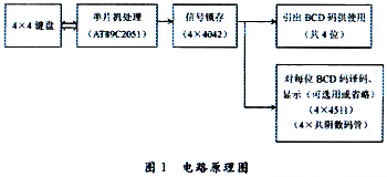
The circuit schematic diagram is shown in Figure 1.

3 Circuit Analysis

The P1 port of AT89C2051 forms a 4×4 matrix keyboard (S0-S15), in which P1.0-P1.3 are used as row lines, and P1.4-P1.7 are used as column lines. The keyboard scanning program can be designed to achieve the preset expectations function (see software design section). Press S0-S9 to generate BCD codes corresponding to decimal numbers 0-9. S10-S13 are used as 4-digit BCD code switching buttons. S14 and S15 are not used yet and do not need to be installed. P3.3-P3.0 are BCD As can be seen from the circuit, the data output line of the code realizes 4-bit BCD code output because of the functional keyboard. Obviously, P3.3-P3.0 is used as a data bus and is connected to four D latches (4042) at the same time. Switching is performed through S10-S13. Only one of the four D latches (U3-U6) is valid at a time and the data of P3.3-P3.0 is "read" and then latched. In fact, S10-S13 controls the status of P3.4 and P3.5 (there are 4 combinations of P3.4 and P3.5) and obtains the corresponding effective values ​​of U3-U6 through the 2-4 line decoder (U2; 74LS139). Signal, Table 1 is the status of each chip corresponding to S10-S13 control. It can be seen that when any one of U3-U6 (for example, U3) is in a valid state and "reads" the P3.3-P3.0 data, the rest (U4 /U5/U6) are in the latched state and retain the original data, so the user can change the desired BCD code output in any bit.

U2 (74LS139) is a 2-4 line decoder. Its functions are shown in Table 1. Its input terminals B and A are connected to P3.4 and P3.5 respectively. The output terminals Y0-Y3 depend on the combination of input terminals. Each combination Only one output terminal (Y0-Y3) outputs an active low level. U3-U6 are D latches. The relationship between pins 5 and 6 determines their working status. According to the information, when the logic potential of pins 5 and 6 is the same, the chip can output D3-D0 data. to Q3-Q0; when the logic potential of pins 5 and 6 is different, the chip is in a state of latching the original data and will not "read in" the current D3-D0 data. Pin 6 of U3-U6 is fixed in the circuit Connect to low potential, and pin 5 is controlled by the output signal of U2 (74LS139). It is not difficult to realize that "the setting of each BCD code can be realized independently". 4511 is a decoding driver. It is connected to a common cathode digital tube to display the decimal number corresponding to the current BCD code of each bit. It is convenient for observation. The display part is very simple and will not be described in detail here. At the same time, the display part is not necessary in the circuit and can be omitted. , the BCD code is derived through J3 and J2. The reason why two linkers are used is for more flexibility and ease of use.

4 The software design

is mainly to implement keyboard processing. The program must confirm which key is pressed, and then transfer to the corresponding processing program for execution. In fact, the program is a complete keyboard scanning program. If the processing subroutine is changed, It can be applied to other control circuits. Detailed procedures and instructions are attached below for reference. Figure 2 is a flow chart.

Simply put, the task of the keyboard scanner is: first confirm whether a key is pressed, then use scanning to determine which row the key is on, and finally find and calculate the specific key by comparing it with the preset 4-line table, thereby converting to the corresponding functional program.

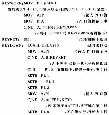
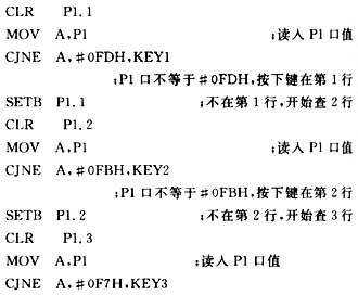
(1) Set the column line to the input state (P1.4-P1.7 is 1), and the row line (P1.0-P1.3) is 0 first, that is, the set P1.7-P1.0 is equal to F0H and Save this status and then read the current P1 port status. It is not difficult to understand that as long as a button (any one) is pressed, the status of P1 port is definitely not the original setting of P1.7-P1.0 equal to F0H. By judging You can achieve the purpose of the first step: first confirm whether there is a button pressed?

(2) Scan step by step starting from the first row (row P1.0) to find and confirm which row the button is on. The scanning method steps are shown in Table 2. Only one row line is 0 at a time. For example, in the first scan, set P1.0 to 0, and P1.1-P1.3 to 1. Obviously, if the button is pressed during the current scan, if it is not the P1.0 row , then the status of the P1 port is always FEH, so the description of Table 2 emphasizes that "only if any comparison of the P1 port is not equal to this value, it means that the current button is in that row" is the meaning. The same is true for the other comparisons. Through this Judgment can be used to find the row number where the key is located.

(3) Four tables KEYVALTAB1-KEYVALTAB4 are defined in the program. The data stored respectively are used to serve the comparison program and indicate the specific positions of the keys in each row. Table 3 lists the correspondence between key labels and comparison data. The rows are stored in R2. The starting value of the number, R0 is used to store the specific location of the key found in each row (the range of R0 is 0-3). The data compared when searching for each row is shown in Table (3). The result can be obtained by simple analysis of reading and writing. Assume that the program first determines that the button is on the first row. Obviously if S0 is pressed, the status of P1.7-P1.0 is 11101110 (S1 is connected to P1.0 and P1.4) , that is, S0→EEH in Table 3.

(4) In the KEYCALCU subroutine, the multiplication by 3 operation is used for the scattered rotation instruction JMP. Note that LJMP is a 3-byte instruction. The function programs corresponding to each button are arranged together to string LJMP, so the multiplication by 3 operation can be correctly mapped to each button. Execute the target function program.

The corresponding processing functions of each key are relatively simple. Just input the corresponding control command corresponding to different keys. For S0-S9, the different states of P3.3-P3.0 are controlled to obtain the corresponding BCD code. For S10-S13 It is to control the status of P3.4 and P3.5 to control U3-U6. Due to space limitations, please refer to the program for details. When the program starts to be executed, it controls the 4-digit BCD code output one by one, and the corresponding digital tubes display in sequence. The initial state is 0001, 0000, 0000, 0000. The 4-digit BCD codes are derived from J3 and J2 respectively, and the digital tube displays 1, 0, 0, 0.

5 4×4 Keyboard Scanner

Keywords:AT89C2051  matrix Reference address:Design of four-bit BCD encoder circuit based on microcontroller

Previous article:Testing and analysis of 8051, ARM and DSP instruction cycles
Next article:Design of four-bit BCD encoder circuit based on microcontroller

Recommended ReadingLatest update time:2024-11-16 23:53

Intelligent clock using AT89C2051
  Functions of the smart electronic clock: 1. Full calendar timing. 2. 12/24 hour conversion. 3. 8-way timing output (can be turned on/off) 4. Error: 15S+1uS 5. Automatic tracking of large and small months, leap years, weeks 2. Adjustment: After power on, the electronic clock displays "1:00". 1. 8-way timing
[Microcontroller]
Intelligent clock using AT89C2051
Design of electronic piano based on AT89C2051
The frequency spectrum of sound ranges from approximately tens to thousands of hertz. If you can use a program to control a certain port of the microcontroller to continuously output "high" or "low" levels, a square wave of a certain frequency can be generated on the port. Connecting the square wave to a speaker can
[Microcontroller]
Design of electronic piano based on AT89C2051
The role of ARM's BUS Matrix
ARM's BUS  Matrix is ​​the cross-linking and arbitration of multiple masters (Core, DMA, etc.) and multiple slaves (internal RAM, APB, external bus, etc.). The purpose is to increase the bandwidth when different hosts access different peripherals, and the other is to simplify  the protocol design of the Bus Master. F
[Microcontroller]
The role of ARM's BUS Matrix
Design of Linear CCD Micron-Level Round Steel Photoelectric Diameter Measuring Instrument
  introduction   There are many traditional methods for measuring the diameter of round steel in the steel industry, such as sampling detection using sizing tools and electromagnetic contact measurement. Measuring with sizing tools is not accurate enough and the speed is very slow; electromagnetic measurement is a c
[Microcontroller]
Design of Linear CCD Micron-Level Round Steel Photoelectric Diameter Measuring Instrument
Latest Microcontroller Articles
  • Download from the Internet--ARM Getting Started Notes
    A brief introduction: From today on, the ARM notebook of the rookie is open, and it can be regarded as a place to store these notes. Why publish it? Maybe you are interested in it. In fact, the reason for these notes is ...
  • Learn ARM development(22)
    Turning off and on interrupts Interrupts are an efficient dialogue mechanism, but sometimes you don't want to interrupt the program while it is running. For example, when you are printing something, the program suddenly interrupts and another ...
  • Learn ARM development(21)
    First, declare the task pointer, because it will be used later. Task pointer volatile TASK_TCB* volatile g_pCurrentTask = NULL;volatile TASK_TCB* vol ...
  • Learn ARM development(20)
    With the previous Tick interrupt, the basic task switching conditions are ready. However, this "easterly" is also difficult to understand. Only through continuous practice can we understand it. ...
  • Learn ARM development(19)
    After many days of hard work, I finally got the interrupt working. But in order to allow RTOS to use timer interrupts, what kind of interrupts can be implemented in S3C44B0? There are two methods in S3C44B0. ...
  • Learn ARM development(14)
  • Learn ARM development(15)
  • Learn ARM development(16)
  • Learn ARM development(17)
Change More Related Popular Components

EEWorld
subscription
account

EEWorld
service
account

Automotive
development
circle

About Us Customer Service Contact Information Datasheet Sitemap LatestNews


Room 1530, 15th Floor, Building B, No.18 Zhongguancun Street, Haidian District, Beijing, Postal Code: 100190 China Telephone: 008610 8235 0740

Copyright © 2005-2024 EEWORLD.com.cn, Inc. All rights reserved 京ICP证060456号 京ICP备10001474号-1 电信业务审批[2006]字第258号函 京公网安备 11010802033920号