1 Test of AT89S51 working mechanism and instruction cycle
The clock of the AT89S51 microcontroller adopts an internal method, and the clock generator divides the oscillation pulse by 2. Since the clock period is twice the oscillation period (clock period = oscillation period P1 + oscillation period P2), and one machine cycle contains 6 clocks, one machine cycle includes 12 oscillation periods of the crystal oscillator. Taking the oscillation frequency of the quartz crystal oscillator as 11.059 2 MHz, the machine cycle of the microcontroller is 12/11.059 2=1.085 1 μs. The instruction cycle of the 51 series microcontroller generally includes 1 to 4 machine cycles. Most instructions are single-cycle instructions, including 2-cycle and 4-cycle instructions.
In order to observe the instruction cycle, perform cyclic setting and clearing operations on the lowest bit of the P1 port of the microcontroller. The source program is as follows:
#include
main() {
while(1) {
P1=0x01;
P1=0x00;
}
}
Use KEIL uVISION2 to compile, link, and generate executable files. When calling Debug in the integrated environment, you can get the disassembly code of the mixed mode of the above source program:
2:main()
3: {
4:while(1)
5:{
6:P1=0x01;
0x000F759001MOVP1(0x90),#0x01
7:P1=0x00;
0x0012 E4CLRA
0x0013 F590MOVP1(0x90),A
8:}
0x001580EDSJMPmain ( C:0003)
The code in italics is the C source program, and the code in regular font is the assembly language code corresponding to the C source program in italics. The first column of each line of assembly code is the location of the code in memory, the second column is the machine code, followed by the compiled and linked assembly language code. All instructions occupy a total of 6 machine cycles (of which "MOV P1(0x90),#0x01" occupies 2 machine cycles, "CLR A" and "MOVP1(0x90),A" each occupies 1 machine cycle, and the last jump The instruction occupies 2 machine cycles), then the total cycle period is 6×machine cycle=6×1.085 1 μs=6.51 μs.

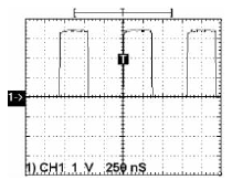
Figure 1 The lowest waveform of port P1
Download the executable file generated by compilation and linking into the Flash of AT89S51 and execute it to get the lowest waveform of the P1 port, as shown in Figure 1. The entire cycle period is 6.1 μs, which is completely consistent with the above analysis.
2 Test of LPC2114 working mechanism and instruction cycle
LPC2114 is an encryptable microcontroller based on the ARM7TDMI core, with zero-wait 128 KB of on-chip Flash and 16 KB of SRAM. The clock frequency can reach 60 MHz (the frequency of the crystal oscillator is 11.059 2 MHz, the clock frequency is set to 11.059 2×4 =44.236 8 MHz, and the on-chip peripheral frequency is 1/4 of the clock frequency, which is the frequency of the crystal oscillator). The ARM7TDMI core improves the execution speed of the instruction stream by using a three-stage pipeline and extensive use of internal registers. It can provide an instruction execution speed of 0.9 MIPS/MHz, that is, the instruction cycle is 1/(0.9×44.236 8)=0.025 12 μs, which is approximately 25ns.
In order to observe the instruction cycle, set the P0.25 pin of GPIO in LPC2114 as an output port, and perform cyclic setting and clearing operations on it. The C source program is as follows:
#include"config.h"
//P0.25 pin output
#defineLEDCON0x02000000
intmain(void)
{//Set all pins to connect to GPIO
PINSEL0 = 0x00000000;
PINSEL1 = 0x00000000;
//Set the LED4 control port as output
IO0DIR = LEDCON;
while(1)
{IO0SET = LEDCON;
IO0CLR = LEDCON;
}
return(0);
}
Use ADS1.2 to compile, link, and generate executable files. When calling AXD Debugger, you can get the disassembly code of the above source program:
main[0xe59f1020]ldrr1,0x40000248
40000224[0xe3a00000]movr0,#0
40000228[0xe5810000]strr0,[r1,#0]
4000022c[0xe5810004]strr0,[r1,#4]
4000 0230[0xe3a00780]movr0,#0x2000000
40000234[0xe1c115c0 [ 0xeaffffffc
] b0x4000023c 40000248[0xe002c000]dcd0xe002c000
The first column of each line of assembly code is the location of the code in memory, the second column is the machine code, followed by the compiled and linked assembly language code. The most critical statements in the loop part are the following three sentences:
4000023c[0xe5810004]strr0,[r1,#4]
40000240[0xe581000c]strr0,[r1,#0xc]
40000244[0xeafffffc]b0x4000023c
在AXD Debugger中,将其调用到RAM中运行程序得到循环部分GPIO的P0.25的输出波形,如图2所示。 从图中可以看出,循环周期中保持为高电平的时间为1350 ns左右,低电平的时间为450 ns左右,即指令“str r0,[r1,#4]”和指令“str r0,[r1,#0xc]”均需350 ns左右,而跳转指令则需100 ns左右。这主要是由于以下原因造成的: ① ARM的大部分指令是单周期的,但是也有一些指令(如乘法指令)是多周期的;② 基于ARM核的微控制器只有加载、存储和交换指令可以对存储器的数据进行访问,这样从存储器读数据或向存储器写数据要增加1个时钟周期;③ 访问片内外设要增加一个外设时钟周期。当然,每个指令还要有1个时钟周期,跳转时要清空流水线还要另加一定的时钟周期。

图2 GPIO的P0.25脚输出波形
为了观察乘法指令,特地采用下述汇编语言进行了实验。首先是没有乘法指令的汇编源程序:
INCLUDELPC2294.INC ;引入头文件
; P0.25引脚控制LED4,低电平点亮
LEDCONEQU0x02000000
EXPORTMAIN
;声明程序代码块
AREALEDCONC,CODE,READONLY
;装载寄存器地址,PINSEL0
MAINLDRR0,=PINSEL0
;设置数据,即设置引脚连接GPIO
MOVR1,#0x00000000
STRR1,[R0]; [R0] ← R1
LDRR0,=PINSEL1
STRR1,[R0]
LDRR0,=IO0DIR
LDRR1,=LEDCON
;设置LED控制口为输出
STRR1,[R0]
;设置GPIO控制参数
LOOPLDRR1,=LEDCON
LEDSETLDRR0,=IO0SET
; LED控制I/O置位,即LED4熄灭
STRR1,[R0]
LEDCLRLDRR0,=IO0CLR
; LED控制I/O复位,即LED4点亮
STRR1,[R0]
;无条件跳转到LOOP
B LOOP
采用ADS1.2进行编译、链接后的汇编代码为:
LOOP [0xe3a01780]movr1,#0x2000000
LEDSET[0xe59f0028] ldrr0,0x40000128
400000fc[0xe5801000]strr1,[r0,#0]
LEDCLR[0xe59f0024] ldrr0,0x4000012c
40000104 [0xe5801000]strr1,[r0,#0]
40000108 [0xeafffff9] bLOOP
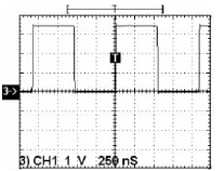
在AXD Debugger中,将其调用到RAM中运行程序得到循环部分的GPIO的P0.25脚输出波形,如图3所示。 从图中可以看出,循环周期中保持为高电平的时间为450 ns左右,低电平的时间为550 ns左右。

图3 GPIO的P0.25脚输出波形2
在上例的LOOP循环部分中加入乘法指令,即将循环部分改为:
LOOP LDRR1,=LEDCON
LEDSETLDRR0,=IO0SET
STRR1,[R0]
MOVR2,#0x0234
MULR2,R1,R2
LEDCLRLDRR0,=IO0CLR
STRR1,[R0]
B LOOP
采用ADS1.2进行编译、链接后的汇编代码为:
LOOP[0xe3a01780]movr1,#0x2000000
LEDSET[0xe59f0030]ldrr0,0x40000130
400000fc[0xe5801000]strr1,[r0,#0]
40000100[0xe3a02f8d]movr2,#0x234
40000104[0xe0020291] mulr2,r1,r2
LEDCLR[0xe59f0024] ldrr0,0x40000134
4000010c[0xe5801000]strr1,[r0,#0]
40000110[0xeafffff7]bLOOP
在AXD Debugger中,将其调用到RAM中运行程序得到循环部分的GPIO的P0.25脚输出波形,如图4所示。 从图中可以看出,循环周期中保持为高电平的时间为550 ns左右,低电平的时间为550 ns左右。与上例比较可知,多出的MUL乘法指令和MOV传送指令共占用100 ns。
综上所述,得出如下结论: 当ARM指令放在RAM中运行时,指令“str r0,[r1,#4]”和指令“strr0,[r1,#0xc]”均需350 ns左右,相当于14个指令周期;指令“ldr r0,0x4000012c”的执行时间为100 ns,相当于4个指令周期;MUL乘法指令和MOV传送指令共占用100ns,相当于4个指令周期;跳转指令共占用100 ns,相当于4个指令周期。
3 TMS320F2812工作机制及指令周期测试
TMS320F2812是TI公司的一款用于控制的高性能和高性价比的32位定点DSP芯片。该芯片最高可在150 MHz主频下工作(本文将其设置到100 MHz),并带有18K×16位0等待周期片上SRAM和128K×16位片上Flash(存取时间为36 ns)。TMS320F2812采用哈佛总线结构,即在同一个时钟周期内可同时进行一次取指令、读数据和写数据的操作,同时TMS320F2812还通过采用8级流水线来提高系统指令的执行速度。
为了观察指令周期,对TMS320F2812的GPIOA0进行循环的置位操作和清除操作。C源程序如下:
#include "DSP28_Device.h"
void main(void) {
InitSysCtrl();/*Initialize system*/
DINT;/*Turn off interrupts*/
IER = 0x0000;
IFR = 0x0000;
InitPieCtrl();/*Initialize PIE control register* /
InitPieVectTable();/*Initialize PIE vector table*/
InitGpio();/*Initialize EV*/
EINT;
ERTM;
for(;;) {
GpioDataRegs.GPADAT.all=0xFFFF;
GpioDataRegs.GPADAT.all=0xFFFF;
GpioDataRegs .GPADAT.all=0xFFFF;
GpioDataRegs.GPADAT.all=0x0000;
GpioDataRegs.GPADAT.all=0x0000;
GpioDataRegs.GPADAT.all=0x0000;
}
}

Figure 4 GPIO pin P0.25 output waveform 3
The most important of these are initializing general-purpose input/output and determining the system CPU clock. The system clock is set to 100 MHz through the PLL, and the source program for initializing InitGpio() is:
#include "DSP28_Device.h"
void InitGpio(void)
{ EALLOW;
//The multiplexer is selected as digital I/O
GpioMuxRegs.GPAMUX.all=0x0000;
//GPIOAO is output, and the rest is input
GpioMuxRegs.GPADIR.all =0x0001;
GpioMuxRegs.GPAQUAL.all=0x0000;
EDIS;
}
By adding a breakpoint at for(;;) in the main program, you can easily find the compiled assembly instructions of the loop part of the main program above:
3F8011 L1:
3F8011761FMOVWDP,#0x01C3
3F8013 2820 MOV@32,#0xFFFF 3F8015 2820 MOV@32,#0xFFFF
3F8017 2820 MOV@32,
#0xFFFF
3F8019 2820 MOV@32,#0xFFFF
3F801B 2820 MOV@32,#0xFFFF
3F801D 2820 MOV @32,#0xFFFF
3F801F 2B20 MOV@32,#0
3F8020 2B20 MOV@32,#0
3F8021 2B20 MOV@32,#0
3F8022 6FEF SBL1,UNC
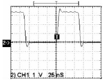
The first column is the location of the program in RAM, the second column is the machine code, and the following is the assembly language program. The instruction "MOV @32,#0xFFFF" causes the GPIO to output a high level, and the instruction "MOV @32,#0" causes the GPIO to output a low level. It contains 6 instructions to make GPIOA0 output high level and 3 instructions to make GPIOA0 output low level. The instruction cycle of the system is 10 ns, so the time to maintain high level in the cycle cycle is 60 ns. By placing the program in H0 SARAM for debugging, the waveform of GPIOA0 can be obtained, as shown in Figure 5. The high level time is exactly 60 ns. Note that since there is a jump after three low levels, the cycle to clear the pipeline is longer.

Figure 5 Waveform 1 of GPIOA0 in TMS320F2812
In order to observe the cycle of the multiplication instruction, modify the C source program in the above loop part to:
for(;;)
{Uint16 test1,test2,test3;
test1=0x1234; test2=0x2345;
GpioDataRegs.GPADAT.all=0xFFFF;
GpioDataRegs.GPADAT.all=0xFFFF;
GpioDataRegs.GPADAT.all=0xFFFF;
test3=test1*test2 ;
GpioDataRegs.GPADAT.all=0x0000;
GpioDataRegs.GPADAT.all=0x0000;
GpioDataRegs.GPADAT.all=0x0000;
}
The assembly instructions of the above program after compilation and linking are as follows:
3F8012L1:
3F80122841MOV*-SP[1],#0x1234
3F8014 2842 MOV*-SP[2],#0x2345
3F8016 761F MOVWDP,#0x01C3
3F8018 2820 MOV@32,#0xFFFF
3F801A 2820 MOV@32,#0xFFFF
3F801C 2820 MOV@ 32,#0xFFFF
3F801E 2D42 MOVT,*-SP[2]
3F801F 1241 MPYACC,T,*-SP[1]
3F8020 9643 MOV*-SP[3],AL
3F8021 2B20 MOV@32,#0
3F8022 2B20 MOV@32 ,#0
3F8023 2B20 MOV@32,#0
3F8024 6FEE SBL1,UNC
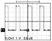
The instruction that makes GPIOA0 high is still 6 instruction cycles (including 1 multiplication instruction). Because the multiplication instruction is also a single cycle, the time to maintain the high level in the cycle cycle is 60 ns. By placing the program in H0 SARAM for debugging, the waveform of GPIOA0 can be obtained, as shown in Figure 6. Among them, the high-level time is exactly 60 ns, and since there are jumps after three low-levels, the pipeline needs to be cleared, and preparations for multiplication are required, the time to maintain the low-level is longer than the time required in Figure 5. long. When observing with a digital oscilloscope, if the waveform observed by using the ×1 gear of the probe is not very ideal, you can use the ×10 gear and adjust the compensation knob of the probe.

Figure 6 Waveform 2 of GPIOA0 in TMS320F2812
4 Comparison of three microprocessors
The first thing to emphasize is that these types of microcontrollers can shorten the instruction cycle by increasing the oscillation frequency of the crystal oscillator, but the oscillation frequency of these controllers has certain limitations. For example, the frequency of the single-chip microcomputer does not exceed 40 MHz, and the frequency of LPC2114 does not exceed 40 MHz. Beyond 60 MHz, the TMS320F2812 has a maximum frequency of 150 MHz. At the same operating frequency, the instruction cycle of ARM instructions is much higher than that of traditional microcontrollers. Because the traditional single-chip microcomputer does not use the pipeline mechanism, and both the ARM core and DSP use the pipeline, but since accessing peripherals and RAM and other memories requires a certain clock cycle, ARM cannot truly achieve single-cycle operation, especially cannot achieve Single-cycle multiplication instructions, while DSP can implement true single-cycle multiplication instructions, which is much faster than ARM microcontrollers.
references
[1] Ma Zhongmei, Ji Shunxin, et al. Design of C language application program for single-chip microcomputer. Beijing: Beihang University Press, 2003. [
2] Xue Junyi, Zhang Yanbin. MCS51/96 series single-chip microcomputers and their applications. Xi'an: Xi'an Jiaotong University Press, 1990.
[3] Zhou Ligong, et al. Fundamentals and Practice of ARM Microcontrollers. Beijing: Beihang University Press, 2005.
[4] Texas Instruments Incorporated. TMS320C28x Assembly Language Tools Users Guide . 2001.
[5] Texas Instruments Incorporated. Software TMS320C28x Optimizing C C++ Compiler Users Guide. 2003.
Previous article:Different initialization of C8051F and 80C51 series microcontrollers
Next article:Home telephone control and alarm system based on AT89C52
Recommended ReadingLatest update time:2024-11-16 16:56

- Popular Resources
- Popular amplifiers
-
 FOUNDRY PROCESS QUALIFICATION GUIDELINES – TECHNOLOGY QUALIFICATION VEHICLE TESTING JEP001-3B
 -
 Semantic Segmentation for Autonomous Driving: Model Evaluation, Dataset Generation, Viewpoint Comparison, and Real-time Performance
 -
 ICCV2023 paper summary: Vision and Robotics
 -
 ICCV2023 Paper Summary: Human-in-the-Loop Computer Vision
 Professor at Beihang University, dedicated to promoting microcontrollers and embedded systems for over 20 years.
- Innolux's intelligent steer-by-wire solution makes cars smarter and safer
- 8051 MCU - Parity Check
- How to efficiently balance the sensitivity of tactile sensing interfaces
- What should I do if the servo motor shakes? What causes the servo motor to shake quickly?
- 【Brushless Motor】Analysis of three-phase BLDC motor and sharing of two popular development boards
- Midea Industrial Technology's subsidiaries Clou Electronics and Hekang New Energy jointly appeared at the Munich Battery Energy Storage Exhibition and Solar Energy Exhibition
- Guoxin Sichen | Application of ferroelectric memory PB85RS2MC in power battery management, with a capacity of 2M
- Analysis of common faults of frequency converter
- In a head-on competition with Qualcomm, what kind of cockpit products has Intel come up with?
- Dalian Rongke's all-vanadium liquid flow battery energy storage equipment industrialization project has entered the sprint stage before production
- Allegro MicroSystems Introduces Advanced Magnetic and Inductive Position Sensing Solutions at Electronica 2024
- Car key in the left hand, liveness detection radar in the right hand, UWB is imperative for cars!
- After a decade of rapid development, domestic CIS has entered the market
- Aegis Dagger Battery + Thor EM-i Super Hybrid, Geely New Energy has thrown out two "king bombs"
- A brief discussion on functional safety - fault, error, and failure
- In the smart car 2.0 cycle, these core industry chains are facing major opportunities!
- The United States and Japan are developing new batteries. CATL faces challenges? How should China's new energy battery industry respond?
- Murata launches high-precision 6-axis inertial sensor for automobiles
- Ford patents pre-charge alarm to help save costs and respond to emergencies
- New real-time microcontroller system from Texas Instruments enables smarter processing in automotive and industrial applications
- About USB2.0 plug-in and switch
- [Atria AT32WB415 Series Bluetooth BLE 5.0 MCU] + Bluetooth communication
- xilinx vivado xdc constraint syntax
- Design and Implementation of Digital Video Conversion Interface Based on FPGA
- [AT-START-F403A Evaluation] VI. FreeRTOS system based on IAR security library (sLib) secondary development mode practice
- About the 2021 E-Sports Championship
- [ST NUCLEO-G071RB Review]——First Look at the Kit
- FPGA Advanced Timing Synthesis Tutorial
- How reliable is Dupont wire???
- Classic Books on Signal Integrity Design

 FOUNDRY PROCESS QUALIFICATION GUIDELINES – TECHNOLOGY QUALIFICATION VEHICLE TESTING JEP001-3B
 ICCV2023 paper summary: Vision and Robotics


 京公网安备 11010802033920号