This paper designs a building wireless video intercom circuit, which uses a single-chip microcomputer as the controller core and connects to peripheral circuits. It transmits video signals through a wireless digital transmission circuit, and can achieve a wireless transmission distance of 50 to 200 meters. The advantage of this design is that it can obtain continuous display of images based on single-shot shooting, and it truly realizes wireless digital transmission of image signals.
1 Overall design plan
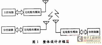
The system structure mainly consists of three parts: the host computer system, the slave computer system and the communication system. These three parts together complete the information exchange between the main controller and the sub-controller to achieve the purpose of building monitoring. The main controller and the sub-controller transmit data and commands through the wireless digital transmission module SRWF. This communication model belongs to a one-to-many communication mode, and its overall block diagram is shown in Figure 1.
The main control chip of the main controller is AT89C51. It obtains the room number to be visited through the keyboard. After confirmation, the single-chip machine will control the opening of the video acquisition chip and the buffer chip to work, and send the data to the digital transmission circuit through the serial port communication under the set communication baud rate. The digital transmission circuit then sends the data through the wireless channel. The main control chip of the slave controller also uses AT89C51. It receives the control information and data information of the main controller through the digital transmission circuit and classifies the received data. If it is a communication address signal sent by the host, the slave controller will read the data in the ringing tone storage circuit and send out a ringing tone. Next, it starts to receive the video signal and displays it through the LCD display circuit. The user can decide whether to have further communication with the main controller through the key control circuit.
2 Hardware Circuit Design
2.1 Circuit Design of Main Controller
The main controller circuit consists of AT89C51 single-chip microcomputer, keyboard scanning circuit, driver and digital display circuit, watchdog circuit, wireless data transmission circuit, etc. The hardware circuit schematic diagram of the main controller system is shown in Figure 2.
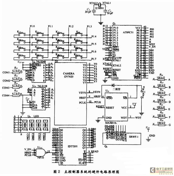
The working process is as follows: First, the keyboard scanning circuit scans the user's key information to obtain the communication address of the slave, and displays the key information through 4 LEDs so that the user can clearly know the slave address he wants to access. The user can confirm and modify the input value by adding, subtracting, and re-entering on the keyboard. When the user presses the confirmation key, the host stores the slave address at this time, turns on the video chip to sample the video signal, and sends the slave address through the wireless digital transmission chip SRWF. After receiving the response signal and ready signal from the slave, the host starts to send data at the set baud rate. Wait for the response signal from the slave every time a frame of data is sent, and send a check frame for each frame of data to ensure the accuracy of data transmission.
2.1.1 Keyboard scanning circuit
The keyboard scanning part uses a 4×4 keyboard, and the scanning level is set through the P1 port. First, one of the lower 4 bits of the P1 port is set to zero, and then the level of the upper 4 bits of the P1 port is read. The lower bit of the P1 port is set to zero, which means that the column line is set low. If a bit is detected as zero in the upper 4 bits of the P1 port, the position of the key can be known through the position of the row and column. There is a jitter problem in the key pressing process. The solution includes hardware encoding keyboard and software encoding. Considering the cost considerations and the high performance of AT89C51, this design uses software encoding to achieve scanning. The keyboard scanning circuit is shown in Figure 2.
2.1.2 LED display circuit
The LED display circuit uses a dynamic display mode, which is composed of a 74LS248 BCD decoder chip and a 74LS138 decoder. The purpose of using 74LS248 is to save I/O port resources so as to control more peripheral chips. The segment selection data of the LED is determined by the segment selection code decoded by 74LS248, and the bit selection data is generated by 74LS138 decoding. When working, the value of the key is first converted into BCD code, and then sent to the 4th bit of the P0 port, but the overall copy of the P0 port will destroy the data of the bit selection port. At this time, the data of the P0 port needs to be corrected, and the bit selection data is also sent to the 4th and 5th bits of the P0 port through the OR logic operation, and then the corrected data is sent to the P0 port. At this time, there are both segment selection data and bit selection data. In order to make the displayed data not flicker, it is necessary to use the visual persistence of the human eye to control the time delay between each data display within 10 ms, so that the displayed numbers will not flicker. The LED display circuit is shown in Figure 2.
2.1.3 Video acquisition and data transmission circuit
The video acquisition circuit is composed of CAMERA 0V 7620 chip and IDT7205. This combination method is adopted because the amount of video data is relatively large, but the working frequency of the single-chip microcomputer is relatively low. If they are directly matched, the two cannot be received normally. Therefore, the buffer chip IDT7205 is added, so that the single-chip microcomputer controls its work to achieve the matching of the data volume and the single-chip microcomputer. IDT7205 is enabled only when the single-chip microcomputer allows reception. If the single-chip microcomputer detects that the VSYN of the video chip jumps up, it will output 1 at the P0.7 port, thereby starting to control IDT7205 to obtain data from the video chip. Before using the SRWF module, the wireless channel, interface type, interface rate, interface parameters, etc. must be set. After the settings are completed, data transmission can be carried out. When the module receives the first data sent by the single-chip microcomputer, it automatically performs wireless network connection and data synchronization. Therefore, the first data will be output from the receiving serial port after a 5-byte time delay, as shown in Figure 2.
2.2 Circuit design of sub-controller
The sub-controller also uses AT89C51 single-chip microcomputer as the microprocessor. The peripheral interface circuit of the sub-controller system consists of a crystal oscillator, LCD image display circuit, key unlocking circuit, watchdog circuit, communication interface circuit, memory, etc. The hardware circuit schematic diagram of the sub-controller system is shown in Figure 3.
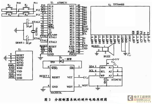
Its working process is: initialize its receiving baud rate and keep in information monitoring state. When receiving the address frame, it will be compared with its own address. If different, discard this frame data and continue to detect. If the same, read the music code stored in the AT24C02 chip, control the speaker to emit music sound through the P2.1 port, and tell the user that a visitor requests to enter the building. When the user presses the answer key on the keyboard, the single chip will send the data received from the wireless digital transmission module to the P0 port for LCD display. When the homeowner sees the image on the LCD, if he knows the visitor, he presses the key to unlock; if he does not know the visitor, he presses the hang-up key to end the video call. The main working chip of the video display circuit is TFT6448B. TFT6448B has its own data latch and does not need to expand the latch chip. After selecting TFT6448B, the control display of TFT6448B can be realized by writing data to the corresponding row, column, control, and data registers of TFT6448B.
3 Software Design
The host is AT89C51 single-chip microcomputer, and the slave is AT89C51 single-chip microcomputer. The data communication baud rate between the host and the slave is set to 9600 B, and each slave has a unique address number to distinguish each slave. The data communication of the single-chip microcomputer is completed by the serial port. Timer T1 is the baud generator. The data transmission format is 1 start bit, 8 data bits, 1 stop bit, and 1 programmable bit (T-B8). Working mode: Set timer T1 to mode 2 and the serial port to working mode 3.
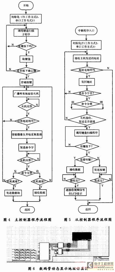
The communication protocol of this system is: the SM2 position of all slaves is 1, and they are in the state of receiving address frames. The host sends an address frame, in which the 8th bit is the address and the 9th bit is the address/data distinguishing mark. The position 1 indicates that the frame is an address frame. After receiving the address frame, all slaves will compare the received address with the address of the local machine. For the slaves with matching addresses, their SM2 position is 0, and the local address is sent back to the host as a response; for the slaves with inconsistent addresses, SM2=1 is still maintained, and the data frame sent by the host is ignored. After the slave finishes sending data, it must send a frame checksum and set the 9th bit to 1 as a mark of the end of the slave data transmission. When the host receives data, it first determines the data reception flag RB8. If RB8=1, it means that the data transmission is over, and compares the checksum of this frame. If it is correct, the correct signal 00H is sent back to command the slave to reset; if it is wrong, the signal OFFH is sent to command the slave to resend the data. If the received frame RB8=0, the data is stored in the buffer and ready to receive the next frame of information. After receiving the response address of the slave, the host confirms whether the address matches. If the address does not match, it sends a reset signal; if the address matches, it clears TB8=0 and starts sending data. After receiving the reset command, the slave returns to the listening address state, otherwise it starts to receive data and commands. The communication program flow chart of the master controller and the slave controller is shown in Figure 4 and Figure 5.
4 System Simulation
Draw the circuit schematic in the ISIS 7.1sp2 software environment of Proteus. The next step is to compile the designed program into machine language in the Keil C51μVision2 integrated development environment. Enter the ISIS of Proteus, click the menu "Debug" with the left mouse button, and select "use romote debugger monitor" to realize the connection debugging between KeilC and Proteus. First, double-click the microcontroller AT89C51 in Proteus, and import the .HEX file generated by programming under KeilC into AT89C51. You can click the full-speed simulation run button in Proteus to view the phenomenon. You can clearly observe the level changes of each pin on the chip. Red represents high level and blue represents low level. If the phenomenon is incorrect, debug the program in KeilC step by step and observe the phenomenon in Proteus. If any step is incorrect, modify the program in that section and debug until the simulation is completely successful.
Press the three buttons on the scanning keyboard in sequence. After all three buttons are entered, the data just pressed will be displayed on the digital tube. The numbers are displayed in the order in which they are pressed. The numbers represent the room number to be visited, such as 504, which means the owner of room 504 is to be visited. The room number will be provided to the microcontroller as the address for multi-machine communication. The simulation results are shown in Figure 6.
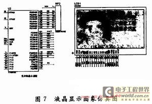
In Proteus, LM4229 is used to replace the TFT6448B chip in the design. The purpose of the simulation is to obtain the encoding method of image display and the monochrome bitmap display function of the LCD. LM4229 determines whether to read data or read status, or write data or write commands through the levels of the three pins CDWRITE READ. Its data pin is 8 bits, which can directly exchange data with the microcontroller. The P2 port is the control end of the LCD display. The simulation results are shown in Figure 7.
5 Conclusion
The visual hedge circuit adopts the design with AT89C51 microcontroller as the core and SRWF-1, CAMERA OV 7620, IDT7205 and other peripheral chips. The hardware circuit diagram and main program flow chart are given in this paper, and the processing of key technologies in the process of software and hardware design is explained. This circuit can fully meet the practical requirements of the building wireless visual intercom circuit for continuous acquisition of image signals, wireless transmission of image signals, display of monochrome bitmaps, and ringing calls. The innovation of this article is to apply low-speed microcontrollers to image signal acquisition with large data volume and short-distance wireless transmission of images. In the design, the real-time processing of image signals will become a direction that needs to be studied in the future.
Previous article:Application of unattended integrated monitoring system
Next article:Trolleybus Rectifier Station Automation Monitoring System
- Popular Resources
- Popular amplifiers
- Molex leverages SAP solutions to drive smart supply chain collaboration
- Pickering Launches New Future-Proof PXIe Single-Slot Controller for High-Performance Test and Measurement Applications
- CGD and Qorvo to jointly revolutionize motor control solutions
- Advanced gameplay, Harting takes your PCB board connection to a new level!
- Nidec Intelligent Motion is the first to launch an electric clutch ECU for two-wheeled vehicles
- Bosch and Tsinghua University renew cooperation agreement on artificial intelligence research to jointly promote the development of artificial intelligence in the industrial field
- GigaDevice unveils new MCU products, deeply unlocking industrial application scenarios with diversified products and solutions
- Advantech: Investing in Edge AI Innovation to Drive an Intelligent Future
- CGD and QORVO will revolutionize motor control solutions
- Innolux's intelligent steer-by-wire solution makes cars smarter and safer
- 8051 MCU - Parity Check
- How to efficiently balance the sensitivity of tactile sensing interfaces
- What should I do if the servo motor shakes? What causes the servo motor to shake quickly?
- 【Brushless Motor】Analysis of three-phase BLDC motor and sharing of two popular development boards
- Midea Industrial Technology's subsidiaries Clou Electronics and Hekang New Energy jointly appeared at the Munich Battery Energy Storage Exhibition and Solar Energy Exhibition
- Guoxin Sichen | Application of ferroelectric memory PB85RS2MC in power battery management, with a capacity of 2M
- Analysis of common faults of frequency converter
- In a head-on competition with Qualcomm, what kind of cockpit products has Intel come up with?
- Dalian Rongke's all-vanadium liquid flow battery energy storage equipment industrialization project has entered the sprint stage before production
- Allegro MicroSystems Introduces Advanced Magnetic and Inductive Position Sensing Solutions at Electronica 2024
- Car key in the left hand, liveness detection radar in the right hand, UWB is imperative for cars!
- After a decade of rapid development, domestic CIS has entered the market
- Aegis Dagger Battery + Thor EM-i Super Hybrid, Geely New Energy has thrown out two "king bombs"
- A brief discussion on functional safety - fault, error, and failure
- In the smart car 2.0 cycle, these core industry chains are facing major opportunities!
- Rambus Launches Industry's First HBM 4 Controller IP: What Are the Technical Details Behind It?
- The United States and Japan are developing new batteries. CATL faces challenges? How should China's new energy battery industry respond?
- Murata launches high-precision 6-axis inertial sensor for automobiles
- Ford patents pre-charge alarm to help save costs and respond to emergencies
- EEWORLD University Hall----Live playback: Introduction to the industrial open source platform based on TI Sitara?AM5708
- The United States is suppressing China's top companies because it is afraid that the Chinese are "too smart"?
- A low-power, wireless sensor network design
- [TI millimeter wave radar evaluation]_6_AWR1843BOOST UART output data analysis 1
- PA Design Principles and Practice - PA Design Based on MRF8P9040N - Personally Tested ADS2011
- Does anyone have the Chinese operating instructions for the Agilent E4408B spectrum analyzer?
- 【IoT Graduation Project. Part 2】STM32+Gizwits AIoT+Laboratory Safety Monitoring System
- Is it necessary to pull up the data line and pull down the clock line in SWD mode for the burning port?
- MSP430 drives MCP4017 digital potentiometer driver debugging record
- [RVB2601-demo analysis and kernel analysis] YOC architecture + three-color indicator light

 MAX4284EEE


 京公网安备 11010802033920号