Electronic transformer is a new type of transformer device that uses modern digital processing and optical fiber communication technology to achieve voltage and current measurement and protection of power system. ADS8344 is an 8-channel, 16-bit, high-precision, low-power A/D conversion chip produced by TI. TMS320LC545 is a 16-bit, low-power, high-speed DSP chip produced by TI. This paper introduces the main features of ADS8344 and gives its interface design with TMS320LC545 in the high-voltage side data processing system of electronic transformer.
introduction
With the rapid development of information technology and computer technology, digital signal processing technology has gradually become a mainstream technology and has been widely used in many fields. Coupled with the increasing maturity of optical fiber communication technology and sensor technology, it is possible to develop new power transformers. The electronic transformer introduced in this article uses Rogowski coils to measure current, uses the principle of capacitive voltage division to measure voltage, uses high-speed and low-power A/D chips and DSP processors to complete real-time processing of high-voltage side data, and then uses E/O conversion and optical fiber as the signal transmission medium to transmit the pulse signal converted from the high-voltage side to the low-voltage side for measurement and protection.
1 Electronic transformer high voltage side data processing system
The data processing system on the high-voltage side of the electronic transformer is mainly composed of four parts: signal preprocessing, A/D conversion, DSP master control and E/O conversion. The signal preprocessing part receives the analog signals measured by various sensor heads and performs some preprocessing on them. For example: the electromotive force induced by the Rogowski coil needs to be converted into a voltage signal proportional to the phase of the primary current by an integrator; the analog signal measured by the sensor head must be regulated, and a certain margin must be considered to make it conform to the allowable input range of the analog channel of the A/D chip. The A/D conversion part mainly converts the analog signal into a digital signal in real time under the control of the DSP master chip. The E/O conversion part modulates the digital signal into an optical pulse signal, which is then transmitted to the low-voltage side by optical fiber.

2 Main Features of ADS8344
2.1 Structural Features of ADS8344
ADS8344 is a high-speed, low-power, 16-bit successive approximation ADC, powered by a single 2.7V to 5V power supply, with a maximum sampling rate of 100kHz and a signal-to-noise ratio of 84dB. It has a serial interface and contains 8 single-ended analog input channels (CH0~CH7), which can also be synthesized into 4 differential inputs. The typical power consumption at 100kHz is 10mV. The reference voltage VREF ranges from 500mV to VCC, and the corresponding input of each analog channel ranges from 0V to VREF. It has its own sample/hold function, uses a 20-pin QSDP package or a 20-pin SSOP package, and has an operating temperature range of -40℃ to +85℃. This chip is suitable for use in battery-powered systems (such as personal digital assistants, mobile communications) and test equipment.
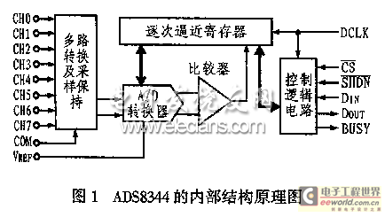
It is mainly composed of a multiplexer, a sample/hold, a reference voltage, an A/D converter, a comparator, a control logic circuit and a successive approximation register (SAR). Its internal structure principle is shown in Figure 1.
2.2 Pinout and Description of ADS8344

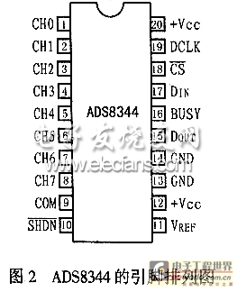
The pin arrangement of ADS8344 is shown in Figure 2, and the pin descriptions are as follows:

CH0~CH7: Input terminals of analog input channels. The 8 single-ended analog input channels can be used as dual-ended differential inputs. The input range of all channels is from 0V to +VREF. Unused input channels should be connected to GND to avoid noise input.
COM: Reference ground for analog input, zero position of single-ended input channel, direct ground or ground potential reference point.
SHDN: Power-down control bit. When it is low, the chip switches to low-power power-down mode.
+VCC: Power input terminal, range is +2.7V~+5V.
DOUT: Serial data output terminal, data is output at the falling edge of DCLK, and when CS is high, the output is in high impedance state.
DIN: Serial data input terminal. When CS is low, the data is latched on the rising edge of DCLK.
DCLK: External clock input terminal, which determines the conversion rate of the chip (fDCLK=24fSAMPLE).
CS: Chip select terminal, when it is at a low level, the chip is selected.
GND: Reference ground.
VREF: Reference power input terminal.
BUSY: Analog-to-digital conversion status output pin. When analog-to-digital conversion is in progress, this pin outputs a low level. When the BUSY terminal generates a falling edge, it indicates that the analog-to-digital conversion is completed and the data output is valid.
2.3 Working Characteristics of ADS8344
The control register of ADS8344 is an 8-bit write-only register. Data is input from the DIN pin. When the microcomputer reads the last conversion result, the control byte of the next conversion channel is written to the DIN pin. It takes 8 DCLK clocks to write the complete control information to the control register. The functions of each bit of the control register are as follows:
S: The start bit of the control byte. When it is high, it indicates that the input byte is valid.
A2~A0: Analog input channel selection bits.
SGL/DIF: Analog channel input mode selection bit. When it is high, it is single-ended input; when it is low, it is dual-ended differential input.
PD1~PD0: Power management selection bits.
(1) Input method of analog channel
The 8 analog input channels of ADS8344 can be set as single-ended input or differential input. In single-ended input, each analog channel inputs +IN signal, and the -IN signal is connected from the COM pin. In double-ended differential input, channels CHO and CH4, CH1 and CH5, CH2 and CH6, CH3 and CH7 are combined into differential input. When the chip enters the hold phase, the differential input signals of +IN and -IN are sent to the internal capacitor array. The voltage range of -IN input is -0.2V to +1.25V, and the voltage range of +IN input is -0.2V to +VCC+0.2V. For example: if the reference voltage is 1.25V and the COM pin is grounded, the voltage range of the single-ended input channel is 0V to +1.25V; if the reference input voltage is 3.3V and the COM pin is connected to +0.5V, the input voltage range of the single-ended input channel is +0.5V to +3.8V.

(2) Power management method
ADS8344 provides flexible power management modes, allowing users to obtain the best power performance at a given throughput rate. The power consumption of the chip can be managed by programming the power bits PD0 and PD1 of the control register. When PD0=0 and PD1=0, it is in automatic shutdown mode. In this mode, the ADS8344 automatically enters low power mode at the end of each conversion. When the next conversion begins, the chip is immediately fully powered on without additional delay, and the first conversion is valid; when PD0=0 and PD1=1, it is in internal clock mode; when PD0=1 and PD1=0, it is in reserved mode; when PD0=1 and PD1=1, it is in full power mode. The chip in this mode is always powered on.
(3) Clock mode
ADS8344 can perform successive conversions by internal clock or external clock, and in both modes, the external clock controls the input/output of chip data. If the user wants to change the clock mode of the chip, an additional conversion cycle is required before the chip switches to the new mode, because the PD0 and PD1 power management selection bits must be written to the ADS8344 control register in advance before the clock mode is switched.
In the external clock mode, the external input clock not only controls the data input/output chip, but also determines the conversion rate of the A/D chip. In the internal clock mode, the ADS8344 chip generates its own clock signal, so the connected microcomputer does not need to generate the SAR conversion clock, and the conversion result can be easily output to the microcomputer.
3 Typical Applications of ADS8344
The electronic transformer high-voltage side data acquisition system introduced in this article uses TMS 320LC545 as the main control chip, and selects ADS8344 chip to realize the real-time acquisition and analog-to-digital conversion of various analog signals output by the sensor head. The main workflow of the high-voltage side data processing system is: receive the analog signal output by the sensor head and pre-process it, then send it to the A/D chip to convert it into a digital signal, and finally convert it into an optical signal through E/O and output it to the optical fiber transmission system.
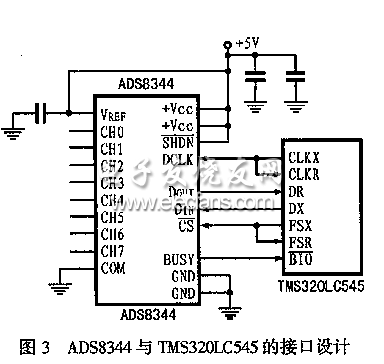
TMS320LC545 is a 16-bit fixed-point low-power digital processor with an operating voltage of +3.3V, 6kB on-chip RAM, 48kB off-chip ROM, and a standard serial port and a buffered serial port. The interface design of the two is shown in Figure 3. The serial port of TMS320LC545 is configured to work in burst mode using the internal CLKX (serial clock) and FSX (frame synchronization clock). The serial port register SPC is set as follows: FO=0, the serial port sends and receives data in 16 bits; FSM=1, the serial port works in character group mode, and each word sent/received requires a frame synchronization pulse FSX/FSR; MCM=0, CLKX uses an external clock, which is sent from the low-voltage side through the optical fiber to ensure that the high and low-voltage side clocks are consistent; TXM=1, FSX is set to output, and a frame synchronization pulse output is generated by the chip each time data is sent. The CS of ADS8344 is connected to the FSX and FSR of TMS320LC545, so that the frame pulse signals of data input and output are generated by DSP; the DCLK of ADS8344 is connected to the CLKX and CLKR of TMS320LC545, so that the synchronous clocks of data input and output come from DSP; the BUSY of ADS8344 is connected to the BIO of TMS320LC545. When BUSY generates a falling edge signal, it notifies the DSP that it can start receiving the conversion results.

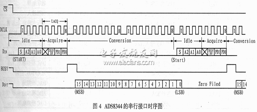
The serial interface timing of ADS8344 is shown in Figure 4. When CS is low, ADS8344 receives serial data sent by DSP chip DX pin through DIN pin and writes it into the control register of A/D chip, which requires 8 DCLK clocks. The first 4 clock cycles are used to receive the start bit and channel selection bit of control byte. When receiving the next 4 control bits, the chip samples the selected channel at the same time, and performs analog-to-digital conversion after sampling. When BUSY generates a falling edge signal, DSP starts to receive the conversion result output by DOUT. 16-bit serial data requires 16 DCLK clocks. When receiving the LSB bit of serial data, the control word of the next channel starts to be input into A/D chip. In this way, ADS8344 needs 25 DCLK clocks to complete a complete data sampling, holding, conversion and output.
4 Conclusion
Electronic transformers have incomparable advantages over traditional electromagnetic transformers and have broad development potential in voltage and current measurement and protection of power systems.
Previous article:Rail transit power monitoring system based on real-time distributed database
Next article:Principle and application of CXT intelligent transmitter
- Popular Resources
- Popular amplifiers
- Molex leverages SAP solutions to drive smart supply chain collaboration
- Pickering Launches New Future-Proof PXIe Single-Slot Controller for High-Performance Test and Measurement Applications
- CGD and Qorvo to jointly revolutionize motor control solutions
- Advanced gameplay, Harting takes your PCB board connection to a new level!
- Nidec Intelligent Motion is the first to launch an electric clutch ECU for two-wheeled vehicles
- Bosch and Tsinghua University renew cooperation agreement on artificial intelligence research to jointly promote the development of artificial intelligence in the industrial field
- GigaDevice unveils new MCU products, deeply unlocking industrial application scenarios with diversified products and solutions
- Advantech: Investing in Edge AI Innovation to Drive an Intelligent Future
- CGD and QORVO will revolutionize motor control solutions
- Innolux's intelligent steer-by-wire solution makes cars smarter and safer
- 8051 MCU - Parity Check
- How to efficiently balance the sensitivity of tactile sensing interfaces
- What should I do if the servo motor shakes? What causes the servo motor to shake quickly?
- 【Brushless Motor】Analysis of three-phase BLDC motor and sharing of two popular development boards
- Midea Industrial Technology's subsidiaries Clou Electronics and Hekang New Energy jointly appeared at the Munich Battery Energy Storage Exhibition and Solar Energy Exhibition
- Guoxin Sichen | Application of ferroelectric memory PB85RS2MC in power battery management, with a capacity of 2M
- Analysis of common faults of frequency converter
- In a head-on competition with Qualcomm, what kind of cockpit products has Intel come up with?
- Dalian Rongke's all-vanadium liquid flow battery energy storage equipment industrialization project has entered the sprint stage before production
- Allegro MicroSystems Introduces Advanced Magnetic and Inductive Position Sensing Solutions at Electronica 2024
- Car key in the left hand, liveness detection radar in the right hand, UWB is imperative for cars!
- After a decade of rapid development, domestic CIS has entered the market
- Aegis Dagger Battery + Thor EM-i Super Hybrid, Geely New Energy has thrown out two "king bombs"
- A brief discussion on functional safety - fault, error, and failure
- In the smart car 2.0 cycle, these core industry chains are facing major opportunities!
- The United States and Japan are developing new batteries. CATL faces challenges? How should China's new energy battery industry respond?
- Murata launches high-precision 6-axis inertial sensor for automobiles
- Ford patents pre-charge alarm to help save costs and respond to emergencies
- New real-time microcontroller system from Texas Instruments enables smarter processing in automotive and industrial applications
- MSP430 MCU printf function transplantation
- Keyence vision camera communicates with Siemens 1500 PLC to achieve grasping correction with the robot
- LSM6DSO(X) sensor driver key code analysis: read_data_polling routine (Part 2)
- Xunwei STM32MP157 development board Linux + MCU learning materials and tutorials summary (manual + video)
- Microchip FAQ | TA100-VAO secure boot and message authentication for CAN FD in ADAS and IVI systems
- C2000 Piccolo MCU F28027F LaunchPad Development Kit
- [MPS Mall Big Offer Experience Season] Unboxing
- [ESP32-Korvo Review] Part 4: Text-to-Speech TTS
- [Silicon Labs Development Kit Review] +PDM Stereo Microphone SPK0641HT4H-1
- Embedded Qt-Realize switching between two windows

 5962-88502012A


 京公网安备 11010802033920号