Traditional virtual instruments consist of a data acquisition board based on the PCI bus that directly utilizes A/D and D/A chips and corresponding software. However, with the rapid development of computer network technology, more and more data needs to be processed, stored and transmitted by computers. Due to the characteristics of general-purpose computers themselves, they are usually not suitable for digital signal processing with high real-time requirements. Therefore, this type of virtual instrument cannot meet the increasingly high requirements of real-time data processing capabilities, data transmission capabilities and data management capabilities put forward by real applications.
At the same time, with the continuous improvement of the cost performance of digital signal processors (DSP), its application areas are rapidly expanding, resulting in the emergence of new virtual instruments based on PCI bus and DSP technology.
Basic framework of the system
The basic framework of the virtual instrument designed by the author based on PCI bus and DSP technology is shown in Figure 1.
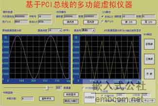
The entire system is implemented based on a modular design concept. The development of this system mainly includes the following steps: 1) Design a motherboard based on the PCI bus, which has its own defined bus connectors, as well as the logic control unit and data buffer storage chip of the entire system; 2) Design the data acquisition module and the data output module; 3) Develop the Windows driver for the PCI motherboard so that the PC can normally identify the board and allocate the required system resources; 4) Develop the program for the DSP data acquisition module of the system's lower computer to realize the acquisition of analog signals and the FFT algorithm processing of data; 5) Develop the control software of the system's upper computer PC to realize data waveform display, port configuration, memory reading and writing, and instrument control functions.
Figure 1 The basic framework of the virtual instrument system

System hardware design
As shown in Figure 1, this virtual instrument system first needs a motherboard based on the PCI bus. The board has a custom bus connector that can be plugged into other data acquisition DSP daughter boards based on the bus. In addition, the board also has the logic control unit of the entire system and the data buffer storage chip; other functional modules are implemented based on the expansion board; the storage and transmission of data between modules can be achieved through dual-port RAM. We choose Cypress's 8K×16b high-speed dual-port RAM chip CY7C025V because its timing matches the DSP timing, which is particularly suitable for high-speed bidirectional transmission of large amounts of data between DSP and PC.
1 Implementation of PCI interface
In the design of PCI bus adapter card, a dedicated PCI interface chip is used to implement PCI interface, and the designer does not need to devote energy to the complex PCI interface function design and verification test. The dedicated interface chip can realize the complete PCI master control module and target interface function, and convert the complex PCI interface into a simple interface. In this design, the universal interface chip PCI9052 of PLX company is selected, which contains read and write FIFOs to match the 32-bit, 33MHz PCI bus with the local bus whose bus width may be narrower than it or whose bus speed may be slower than it. PCI9052 has a maximum of 5 local address spaces and 4 chip selects. Figure 2 is the signal interface module diagram of PCI9052.
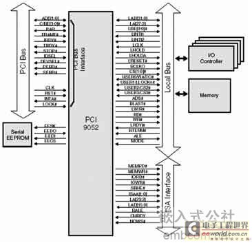
Figure 2 PCI9052 signal interface
The data source of PCI allocated resources is realized through the external EEPROM. According to the requirements of the PCI9052 interface chip, an EEPROM supporting a three-wire serial interface from Microchip is selected. During power-on, the PCI RST# signal resets the PCI9052 internal registers. The PCI9052 also outputs a local reset signal (LRESET#) and checks whether there is an external EEPROM. If it exists and the first 16-bit word is not FFFFH, the PCI9052 loads the data in the EEPROM into the internal registers of the PCI9052; otherwise, the default value is used. The PCI9052 configuration register can only be written by the EEPROM or the PCI host processor. During EEPROM initialization, the PCI9052 responds to PCI target access with the RETRY signal. Figure 3 shows the connection circuit diagram of the EEPROM (93CS46) and PCI9052 in this design.
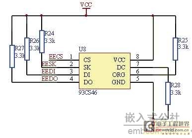
Figure 3 Connection circuit diagram of EEPROM and PCI9052
The main information configured in the EEPROM includes: device identification number, vendor code, size of four local bus spaces and base address of the space, etc. The configuration information can be written into the configuration EEPROM in advance through a programmer, or the EEPROM can be operated with PLXMon after the system starts.
2 Implementation of system control logic
Since the CPLD device can save the internal program of the chip after power failure, there is no need for tedious repeated burning, so this design uses Altera's CPLD device as the logic control of the PCI interface chip and storage chip. Considering the need to use 16 local address/data lines and 22 control signal lines, and to reserve some I/O pins for the data acquisition circuit, it was finally decided to use the EPM3128 in the 144-pin TQFP package.
In this system, the main functions of EPM3128 are to realize the address decoding of PCI Local, the address decoding of each DRAM control by DSP Local, and the decoding of the state of the function selection switch on the board, so as to realize the configuration of system functions and the logic decoding of the control signals of each chip. All decoding work is realized by VHDL programming language. The synthesis and compilation work is completed in Altera's QuartusII integrated compilation environment.
3 Implementation of data acquisition circuit
The data acquisition circuit is the key to this system. The quality of the data acquisition circuit design will directly affect the performance of this system. In order to achieve the configurability and scalability of the system function, the data acquisition module is designed in a configurable mode and plugged into the bus interface motherboard to realize the data acquisition of external signals. The data acquisition module consists of a high-speed 16-bit ADC (LTC1608) and a high-performance DSP chip ( TMS320C6713 ). The parallel digital interface of LTC1608 can easily communicate with a variety of DSPs including TMS320C6713, and can be connected to 3V or 5V logic.
Due to the high requirements for acquisition accuracy, before the signal enters the ADC, a series of processing is required on the analog signal to ensure the reliability of the signal: the analog signal first passes through a voltage follower operational amplifier to increase the input impedance, then undergoes voltage proportional amplification and first-order RC low-pass filtering, and finally is input into the ADC.
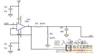
Figure 4 Schematic diagram of input signal processing circuit
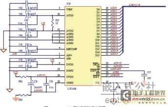
Figure 5 LTC1608 A/D chip pin connection circuit diagram
The specific signal processing circuit is shown in FIG4 and FIG5.
System software design
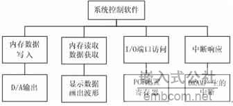
As shown in Figure 1, after the hardware design is completed, software support is still needed to make the entire system work. The software includes PCI device drivers, data processing algorithm programs, and system control software.
1 Device Driver Design
Device drivers do not exist independently, but are part of the kernel of the relevant operating system, so you need to have a certain understanding of the operating system. Windows 2000 operating system is a 32-bit multi-tasking non-real-time operating system. The operation of the entire system bottom layer and the user's right to interact with the hardware are shielded, and the operating system must uniformly manage device drivers and other kernel access to enable application software to access hardware. When designing and using PCI devices, it is often necessary to access system resources in software, so only by compiling device drivers can you achieve full access to PCI bus devices.
An application makes a Win32 call for device I/O, which is received by the I/O system service. The I/O manager constructs an appropriate I/O request packet (IRP) from this request. In the simplest case, the I/O manager simply passes the IRP to a device driver, which interacts with the hardware and completes the processing of the IRP. The I/O manager returns data and results to Win32 and the user application. It is common for an IRP to be processed by a layered stack of device drivers. Each driver divides the request into simpler requests. The highest-level driver (such as the file system driver) knows how the file is represented on the disk, but does not know the details of how to get the data; the middle-level drivers further process the request; and the lowest-level drivers actually interact with the hardware.
The hardware driver development tool selected for this design is a driver integrated development kit (DriverStudio) provided by Compuware. The DriverWorks tool can be used to generate a PCI bus driver framework, and then implement input and output processing in WDM, which can be achieved using the KIoRange class.
In the process of generating the driver framework, we can declare the resources to be used in the driver through the wizard; by calling the Initialize() function of the KIoRange class, we can initialize the resources (map the PCI local space); the application layer sends commands to the driver through the DeviceIoControl function to call the member function of KIoRange to implement the application layer's processing of the I/O space. Developing a windows driver for a PCI motherboard is to enable the PC to normally identify the card and allocate the required system resources.
2 Implementation of FFT algorithm
The system needs to develop and implement a program for collecting analog signals and performing FFT (Fast Fourier Transform) algorithm processing on the data for the DSP data acquisition module.
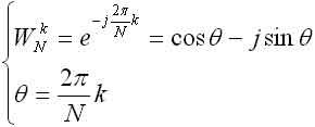
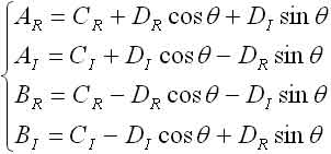
As a general case, assume that x(n) and X(k) are both complex numbers, because from the actual calculation process, there is no difference between real numbers and complex numbers. The only difference is that the imaginary part of a real number is zero and the expression is simpler. All calculations in the operation process are performed on real numbers. If the signal or spectrum is a complex number, the final calculation result is combined into a complex component. The basic unit of FFT operation is the "butterfly unit", and the basic form of the butterfly operation is shown in the following formula:

The operations of all butterfly units can be uniformly expressed as
(1)

Previous article:Anti-interference Design in Digital Image Processing System Based on DSP
Next article:Discussion on the bioelectric signal acquisition solution based on SiC integration technology
- Popular Resources
- Popular amplifiers
- Molex leverages SAP solutions to drive smart supply chain collaboration
- Pickering Launches New Future-Proof PXIe Single-Slot Controller for High-Performance Test and Measurement Applications
- CGD and Qorvo to jointly revolutionize motor control solutions
- Advanced gameplay, Harting takes your PCB board connection to a new level!
- Nidec Intelligent Motion is the first to launch an electric clutch ECU for two-wheeled vehicles
- Bosch and Tsinghua University renew cooperation agreement on artificial intelligence research to jointly promote the development of artificial intelligence in the industrial field
- GigaDevice unveils new MCU products, deeply unlocking industrial application scenarios with diversified products and solutions
- Advantech: Investing in Edge AI Innovation to Drive an Intelligent Future
- CGD and QORVO will revolutionize motor control solutions
- Innolux's intelligent steer-by-wire solution makes cars smarter and safer
- 8051 MCU - Parity Check
- How to efficiently balance the sensitivity of tactile sensing interfaces
- What should I do if the servo motor shakes? What causes the servo motor to shake quickly?
- 【Brushless Motor】Analysis of three-phase BLDC motor and sharing of two popular development boards
- Midea Industrial Technology's subsidiaries Clou Electronics and Hekang New Energy jointly appeared at the Munich Battery Energy Storage Exhibition and Solar Energy Exhibition
- Guoxin Sichen | Application of ferroelectric memory PB85RS2MC in power battery management, with a capacity of 2M
- Analysis of common faults of frequency converter
- In a head-on competition with Qualcomm, what kind of cockpit products has Intel come up with?
- Dalian Rongke's all-vanadium liquid flow battery energy storage equipment industrialization project has entered the sprint stage before production
- Allegro MicroSystems Introduces Advanced Magnetic and Inductive Position Sensing Solutions at Electronica 2024
- Car key in the left hand, liveness detection radar in the right hand, UWB is imperative for cars!
- After a decade of rapid development, domestic CIS has entered the market
- Aegis Dagger Battery + Thor EM-i Super Hybrid, Geely New Energy has thrown out two "king bombs"
- A brief discussion on functional safety - fault, error, and failure
- In the smart car 2.0 cycle, these core industry chains are facing major opportunities!
- The United States and Japan are developing new batteries. CATL faces challenges? How should China's new energy battery industry respond?
- Murata launches high-precision 6-axis inertial sensor for automobiles
- Ford patents pre-charge alarm to help save costs and respond to emergencies
- New real-time microcontroller system from Texas Instruments enables smarter processing in automotive and industrial applications
- How to set up the serial port of 51 microcontroller to communicate with PC
- Step-by-step considerations for designing wide-bandwidth, multichannel systems
- DSP Digital Image Design Report
- Digital Integrated Circuits—Circuits, Systems, and Design (Second Edition)
- Two-color graphic details capacitors and application circuits
- JY02A(居逸電子)馬達驅動IC動作原理
- What is Q
- [Construction Monitoring and Security System] XI. Kaluga MQTT connects to OneNET
- Some basic principles of wireless communication
- 【RT-Thread Reading Notes】(0) Some basic concepts and understanding of threads

 EL5111AIYEZ-T7


 京公网安备 11010802033920号