This article will first highlight some of the automotive design/reliability constraints, then evaluate digital cluster architectures and how memory subsystem trade-offs affect performance, reliability, and cost for future projects.
Challenges of Digital Instrument Cluster Design
数字式仪表群必须支持高性能实时处理需求(就像现有的消费级显示平台),同时显著提升设计的长期可靠性。汽车市场的OEM厂商(原始设备制造商)、一级供应商和客户绝不会将显示故障视为消费级电话或个人电脑经常发生的小问题。新的数字式仪表群需要打造一种简单易用、排除干扰的信息环境,从而促进安全驾驶,这类产品必须确保出色的性能水平以及长期的可靠运行,同时承受苛刻而恶劣的工作环境(例如,-40~+105℃的极端温度范围)。汽车行业在环境、安全和质量方面的这些严苛要求导致开发周期极为漫长,有时开发一项车辆显示技术需要耗时3年,甚至更久。
The planning, design and verification process of automotive design is extremely systematic in order to identify and eliminate operational or reliability problems. In this process, automotive designers usually choose electronic component suppliers that develop products using strict quality design methodologies such as TS16949 and meet the demanding AEC-Q100 standards of the Automotive Electronics Council (AEC).
Once a supplier launches a production system, component suppliers must continuously monitor its internal and external reliability performance and take corrective actions when necessary to ensure that the defective parts per million (dppm) rate is reduced to zero. OEMs and Tier 1 suppliers also expect their supply base to provide long-term product support and availability; once an automotive embedded system is deployed, it is costly to stop, and sometimes it is impossible to revalidate a design to support a short-lived component. In some cases, the cost of revalidation can be as high as hundreds of thousands of dollars.
The increasing use of graphic content in digital instrument clusters has led to more sophisticated information displays, which require not only higher performance levels, but must still reliably accomplish the basic goal of informing the driver of basic vehicle and safety information. For example, digital instrument clusters must provide vehicle status information in a near-instantaneous manner after the vehicle is started, typically displaying important transmission gear information (i.e., P, R, D, 1, 2, 3) on the TFT screen in less than a second. This requires the instrument cluster to be able to start instantly, and to achieve this, designers need to carefully study the performance at the key system and component levels. Even seemingly simple information such as providing a low tire pressure warning before the vehicle is started can proactively reduce potential safety issues in advance.
The transition from analog to digital instrument clusters is exciting, but as mentioned above, it also brings increased complexity, forcing designers to find innovative solutions to meet demanding system requirements such as real-time display performance, long-term high reliability, and significant cost reduction.
We will examine how to provide this essential information in a reliable and cost-effective manner.
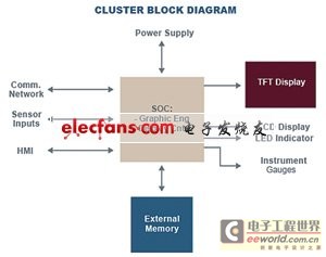
Figure 1 is a schematic diagram of an advanced digital instrument cluster. The vehicle's central system-on-chip (SOC) obtains input data through its communication network and internal or external memory, and outputs it to the TFT display. The system architecture used in the digital instrument cluster is similar to many consumer-grade high-performance display platforms.

Figure 1 Schematic diagram of advanced digital instrument cluster
Both automotive and consumer display platforms require large-capacity memory to support their huge digital content; the emergence of 3D graphics content, 32-bit color, high resolution and large display screens in today's automotive designs has led to memory densities of up to 2Gb.
To create a rich content display system, the content usually includes a large character set, multiple fonts, graphic images, and multi-language extension support. The digital instrument cluster frame buffer is generated and displayed according to industry standard technology. The SOC display controller renders a frame on the system display, while the SOC/graphics engine accesses internal or external memory to obtain, process, and save the next set of data in the frame buffer for subsequent display. Today's SOCs need to access reliable code and data residing in external memory with high bandwidth to ensure fast system startup and high-speed real-time processing.
Digital cluster architecture and memory subsystem trade-offs
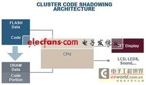
Memory architecture and design implementation can impact the performance level and reliability of an embedded system. Several memory architectures will be evaluated to illustrate some of the performance/cost trade-offs that can be achieved with current technology. First, Figure 2 provides a simplified overview of a standard code-mapped memory architecture that is commonly used in high-performance embedded display systems.

Figure 2 Standard code-mapped memory architecture
The system controller or general processing unit (GPU) is highly integrated and includes a graphics engine, display controller, limited RAM and flash memory options, while still providing external memory interfaces to meet the needs of digital instrument clusters for high performance and high density memory. External memory is divided into two standard products: DRAM and flash. The startup of an embedded system is mainly divided into three steps: first, the code/data is mapped from flash to DRAM, then the processor, DRAM and other key components are initialized, and finally the application is executed. Once the code execution begins, useful information will be displayed. This architecture has several key features. The high-speed access capability of SOC/DRAM can improve the performance of real-time processing functions. The initial system startup time is mainly determined by the mapping and initialization time, and the mapping time depends on the SOC/Flash access bandwidth and the data density transferred from flash to DRAM.
As mentioned earlier, high-end digital instrument clusters must provide the current vehicle status in a near-instantaneous form after the vehicle is started. Gear information (i.e., P, R, D, 1, 2, 3) must usually be displayed on the TFT screen within one second. This requires flash memory to support high-speed access, ultra-high storage density, and long-term data integrity to meet basic design and quality requirements, while also requiring procurement responsibilities to ensure long-term stable supply of products.
Currently, flash memory vendors offer a variety of non-volatile memory (NVM) technologies, of which the two most widely used technologies are NOR and NAND flash. The two have different performance characteristics in various aspects, such as access capabilities, reliability, product life cycle and cost. Automotive SOCs usually support multiple interface configurations to access external parallel and serial NOR flash, while NAND flash interfaces are gradually gaining more and more widespread support.
Note that there is a dynamic variable in the SOC NAND interface that determines the level of ECC support required, especially given the rapid transition of NAND to photolithography. On the NOR side, page mode and synchronous NOR flash will continue to meet the stringent requirements of the automotive industry. For example, new high-end digital cluster designs such as the Chevrolet Volt's E-Flex cluster use Freescale's MPC5121e SOC and Spansion's S29GL512N flash. Spansion GL page read access technology supports high-speed read access with data throughput rates of up to 80MB/s, which is exactly what the Volt E-Flex cluster needs to display the transmission gear position (i.e., P, R, D, 1, 2, 3) within one second of starting the car.
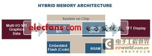
Continuous innovations from automotive chipset and flash memory suppliers have led to a new, highly cost-effective hybrid digital instrument cluster architecture (see Figure 3). The system controller (Freescale Spectrum) and flash memory (Spansion Multi I/O SPI) can optimize the TFT display architecture and provide a more cost-effective entry-level instrument cluster solution. The system controller executes code through embedded flash memory while loading graphic data from external flash memory using a high-bandwidth multi-I/O SPI protocol. The graphic data is processed and saved in the internal frame buffer and then displayed directly on the TFT screen. This bold and innovative hybrid architecture does not require external DRAM memory, which not only meets the performance and reliability requirements of the system, but also optimizes costs.

Figure 3 Hybrid memory architecture
Note that this application architecture requires hundreds of millions of read cycles, which affects the availability of technologies such as NAND. Currently, NAND devices experience more bit disturb errors when used in applications with medium to high read cycles.
The new Multi-I/O SPI communication protocol can be used for data transfer between the system controller and the external SPI Flash memory. The Multi-I/O SPI is based on the popular Serial Peripheral Interface (SPI), and its access performance can be configured to support 1-4 data connections. This feature can increase the access capability of the SPI from less than 10Mb/s to about 40Mb/s. Automotive chipset and flash memory suppliers such as Freescale and Spansion can provide a variety of standard products to ensure that designers can take full advantage of the improved access bandwidth of the Multi-I/O SPI, thereby achieving better cost control while creating a digital instrument cluster with excellent performance. In some cases, two quad I/O SPIs can be used to support continuous throughput rates of up to 80 MB/s.
Spansion's multi-I/O SPI FL flash memory series still supports a low pin count serial interface and supports higher read bandwidth, comparable to current multi-pin count flash memory devices. Spansion's SPI FL series also meets the requirements of medium and high storage density and long-term data integrity, and can maintain normal operation in working environments up to 105°C, while meeting AEC-Q100 standards.
Previous article:Mobile media sources create a new generation of rear-seat entertainment system - mobile living room This article will first highlight some of the automotive design/reliability constraints, then evaluate digital cluster architectures and how memory subsystem trade-offs affect performance, reliability, and cost for future projects.
Next article:
- Popular Resources
- Popular amplifiers
- Molex leverages SAP solutions to drive smart supply chain collaboration
- Pickering Launches New Future-Proof PXIe Single-Slot Controller for High-Performance Test and Measurement Applications
- CGD and Qorvo to jointly revolutionize motor control solutions
- Advanced gameplay, Harting takes your PCB board connection to a new level!
- Nidec Intelligent Motion is the first to launch an electric clutch ECU for two-wheeled vehicles
- Bosch and Tsinghua University renew cooperation agreement on artificial intelligence research to jointly promote the development of artificial intelligence in the industrial field
- GigaDevice unveils new MCU products, deeply unlocking industrial application scenarios with diversified products and solutions
- Advantech: Investing in Edge AI Innovation to Drive an Intelligent Future
- CGD and QORVO will revolutionize motor control solutions
- Innolux's intelligent steer-by-wire solution makes cars smarter and safer
- 8051 MCU - Parity Check
- How to efficiently balance the sensitivity of tactile sensing interfaces
- What should I do if the servo motor shakes? What causes the servo motor to shake quickly?
- 【Brushless Motor】Analysis of three-phase BLDC motor and sharing of two popular development boards
- Midea Industrial Technology's subsidiaries Clou Electronics and Hekang New Energy jointly appeared at the Munich Battery Energy Storage Exhibition and Solar Energy Exhibition
- Guoxin Sichen | Application of ferroelectric memory PB85RS2MC in power battery management, with a capacity of 2M
- Analysis of common faults of frequency converter
- In a head-on competition with Qualcomm, what kind of cockpit products has Intel come up with?
- Dalian Rongke's all-vanadium liquid flow battery energy storage equipment industrialization project has entered the sprint stage before production
- Allegro MicroSystems Introduces Advanced Magnetic and Inductive Position Sensing Solutions at Electronica 2024
- Car key in the left hand, liveness detection radar in the right hand, UWB is imperative for cars!
- After a decade of rapid development, domestic CIS has entered the market
- Aegis Dagger Battery + Thor EM-i Super Hybrid, Geely New Energy has thrown out two "king bombs"
- A brief discussion on functional safety - fault, error, and failure
- In the smart car 2.0 cycle, these core industry chains are facing major opportunities!
- The United States and Japan are developing new batteries. CATL faces challenges? How should China's new energy battery industry respond?
- Murata launches high-precision 6-axis inertial sensor for automobiles
- Ford patents pre-charge alarm to help save costs and respond to emergencies
- New real-time microcontroller system from Texas Instruments enables smarter processing in automotive and industrial applications
- Calculation of wireless communication distance
- This year, friends in the RF field, please come and discuss.
- XMC4800 Review (V) Simple CAN to USB Converter
- kicad-age_12-layer_ciaa_acc
- Goodbye 2019, Hello 2020 + Standing at the Crossroads of Life
- 【GD32307E-START】02-Drawing of mechanical dimension drawings
- Xunwei i.MX6ULL Terminator Buildoot file system construction chapter buildroot file system test
- Spectrum Analysis Series: Why do we need a preselector?
- NXP LPC824
- Servo System, edited by Zeng Lesheng and Shi Miaohe, complete version with cover.pdf

 AD8099ARDZ


 京公网安备 11010802033920号