When designing power management circuits, it is helpful to have a basic understanding of heat transfer before examining the issue of heat dissipation. First, heat is a form of energy that is transferred due to a temperature difference between two systems. Heat transfer occurs in three ways: conduction, convection, and radiation. Conduction occurs when a high-temperature device touches a low-temperature device. The high-amplitude atoms of the high-temperature material collide with the atoms of the low-temperature material, increasing the kinetic energy of the low-temperature material. This increase in kinetic energy causes the temperature of the high-temperature material to rise and the temperature of the low-temperature material to drop.
In convection, heat transfer occurs in the air surrounding the device. In natural convection, an object heats the surrounding air, which expands as it heats, creating a vacuum, causing cold air to replace the hot air. This creates a circulating airflow that continuously transfers heat from the device to the surrounding air. Another form is forced convection, such as a fan actively blowing cold air, which accelerates the replacement of warm air. Radiation occurs when an object sends electromagnetic waves (thermal radiation) to the surrounding environment. Radiated heat does not require a medium to transfer (heat can be radiated through a vacuum). In PCBs, the main method of heat transfer is conduction, followed by convection.
The mathematical model for heat transfer by conduction is given by the following equation:


Where H is the heat transfer rate in J/s, K is the thermal conductivity of the material, A is the area, (TH–TL) is the temperature difference, and d is the distance. Heat conduction increases when the contact area between the interfaces increases, the temperature difference increases, or the distance between the interfaces decreases. Heat transfer can be simulated as a circuit by equating the energy source (heat source or H in the previous equation) to the current source, the temperature difference between the high temperature device and the low temperature device to the voltage drop, and the (K×A/d) part as the thermal conductivity or the reciprocal (EQ2) to the thermal resistance in °C/W. Thermal resistance is usually expressed with the symbol θ or Rθ or simply RA-B, where A and B are the two devices where heat transfer occurs. Rewriting the equation for the heat transfer rate using circuit simulation gives the following result:

The simulation can be further extended to describe another thermal property of the device, called thermal capacitance. Just as thermal resistance is modeled as resistance, thermal capacitance (CT, in J/°C) can be modeled as capacitance. Thermal capacitance is connected in parallel with thermal resistance to obtain thermal impedance (ZT). Figure 1 shows a simplified RC model for conduction heat transfer. The energy source is modeled as a current source and the thermal impedance is modeled as CT in parallel with RT.
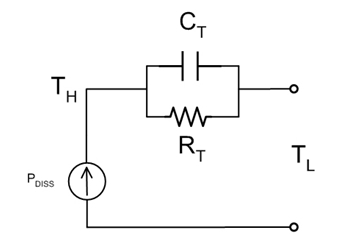
Figure 1. Simplified thermal impedance model.
In a circuit, every thermal interface has a thermal impedance. Thermal impedances vary by material, geometry, size, and orientation. The thermal impedance of a system (or circuit) has a total thermal impedance to ambient temperature that can be decomposed into a parallel and series combination of the thermal impedances of each component in the circuit. For example, in a semiconductor device, the total thermal impedance between the die (also called the junction) and the surrounding air (called the thermal impedance), the thermal impedance from junction to ambient (ZJ-A), will be the sum of the individual thermal impedances of each individual material in the structure.
Consider a discrete MOSFET mounted on a PCB. The steady-state thermal impedance (or thermal resistance RJ-A) is the sum of the thermal resistance from junction to device case (RJ-C), the thermal resistance from device case to heat sink (RC-S), and the thermal resistance from heat sink to air (RS-A). (RJ-A=RJ-C+RC-S+RS-A). In addition, there can be parallel heat dissipation paths, such as from the MOSFET junction through the device case to the PCB, and then from the PCB to the ambient temperature.
Typically, semiconductor manufacturers specify the thermal resistance from junction to device case. RC-S and RS-A, on the other hand, depend primarily on the properties of the heat sink and PCB. Many factors affect the thermal resistance RC-A or RC-S, including the number of PCB layers, the number of vias to secondary surfaces, the proximity to other devices, and the airflow rate. Typically, RJ-A is listed in the device datasheet, but this number is derived under specific test board conditions and is therefore only applicable to comparisons between devices measured under the same conditions.
Thermal resistance (RJA) is an important parameter for electronic components because it is an indicator of how well the device dissipates heat (based on ambient conditions and PCB layout). In other words, RJ-A can help us estimate the operating junction temperature based on ambient conditions and power consumption.
Heat dissipation in switching power supplies
A typical example of thermal considerations in power management circuits can be seen in the LM3554 circuit from National Semiconductor shown in Figure 2. This device is an inductive boost converter targeted at high-power flash LEDs in cell phone applications. The LM3554 is a good test vehicle because it is a small device (1.6mm ( 1.6mm ( 0.6mm)) and can provide up to 6W of output power (1.2A flash current in a 5V LED). Even with its 85% efficiency, relatively large output power capability, and tiny 16-bump μSMD package, the device is subject to high operating temperatures.
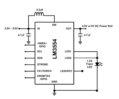
Figure 2. National Semiconductor's LM3554 flash LED driver test circuit.
The initial heat dissipation effect in the LM3554 is primarily an increase in the on-resistance of the device switches and a change in the device threshold. In extreme cases of overheating, the device may hit the thermal shutdown threshold and shut down. Knowing the exact RJ-A can help determine the junction temperature of the device during power operation and ensure that the circuit reliably completes the application requirements as expected.
In the possible case, the device is able to have an input voltage of 3.6V, an LED voltage of 3.6V, and an LED current of 1.2A. In this case, the converter boosts the output voltage to 300mV above VIN. This provides a net voltage of 300mV for the device's two parallel current sources, which are responsible for regulating the LED current.
The total power dissipation of the device will be the sum of the power dissipated by the synchronous PFET, NFET, and the two current sources. The power dissipated by the PFET and NFET is in the resistor components, so the RMS current must be used to accurately estimate the power dissipation. This current is simply the RMS inductor current multiplied by the percentage of the switching period (the on-time of the NFET and PFET). If the converter efficiency is known, the duty cycle can be calculated using the following equation:

For our case, VOUT = VLED + 300mV, and the efficiency is about 90%. This works out to a PFET duty cycle (1-D) of 83% and an NFET duty cycle of 17%. The RMS inductor current equation is:

Where ΔIL is the peak-to-peak inductor current, approximately 140mA in our example, and ILDC is the average inductor current calculated by ILED/(1-D).
The total power dissipation in the switch becomes 45mW for the NFET (RDS_ON = 125mΩ) plus 265mW for the PFET (RDS_ON = 152mΩ). In addition, the power dissipation in the current source is 300mV × 1.2A = 360mW, making the total internal power dissipation 668mW. The RJ-A given in the datasheet is 60℃/W and is from a 4-layer JEDEC test board (see JESD 51-7 for details). Using this RJ-A, the predicted junction temperature is 83.4℃ at TA = 50℃. This will not be a problem for the device because it is below the thermal shutdown threshold of 150℃ and below the maximum operating junction temperature of 125℃ specified in the LM3554 datasheet.
In another case, the LM3554 can be set to output +5V constantly during the same flash pulse. The net voltage of the 300mV current source now becomes 5V–3.6V=1.4V, resulting in a current source power dissipation of 1.68W. Assuming the device is still 90% efficient when providing 5V at 1.2A, the duty cycle is 35.2%, resulting in a ΔIL of 288mA for a DC inductor current of 1.85A. The NFET power dissipation is now 151mW and the PFET power dissipation is 338mW. The total internal power dissipation of 2.169W will result in a high core temperature of 180°C at TA=50°C, which is 30°C above the thermal shutdown threshold and 55°C above the maximum operating junction temperature.
In reality, the device will not be mounted on a 4LJEDEC test board, but on a PCB with a different routing plane, close to other components consuming power, and with a different number of vias to lower layers. All of these application variables, plus many others, can significantly affect RJ-A, reducing the accuracy of the junction temperature calculation.
Measuring thermal impedance (RJ-A and CJ-A)
What is needed is an accurate RJ-A that represents the actual circuit. There are several ways to measure RJ-A, one method is to use the thermal shutdown threshold, set to +150°C. To measure RJ-A using this method, we can operate the LM3554 at a known power dissipation (PDISS) and then slowly increase the ambient temperature until the device shuts down. The device has an internal flag that can be set through the I2C compatible interface that returns a '1' when the thermal shutdown threshold is hit. The RJ-A obtained using this method will be:

Another method is to use an ESD protection diode in the device and measure its VF vs. temperature. This method is slightly more complicated, but the results will be more accurate because the VF can be characterized over the entire temperature range. Most semiconductor devices have an ESD diode on each pin, with its anode connected to GND and its cathode connected to the respective pin.
To test the LM3554, we can look at the LEDI/NTC pin and pull a small current (< 10mA) from it while varying the temperature. The absolute maximum rating for each pin is -0.3V minimum, but that is due to the VF of the ESD diode at its maximum junction temperature of +150°C. If we limit the current to less than 10mA, we can look at the VF of the diode without damaging the device and adding any self-heating. Measurements from this pin produce a linear response from +25°C to +125°C, with a slope of approximately 1.3mV/°C. Once this is done, the device can be operated with known power dissipation while measuring the VF of the selected ESD diode. When the VF reaches steady state, RJ-A will be:

Where VF@TA is the VF of the ESD diode when TJ=TA, and VF@SS is the VF of the ESD diode after TJ reaches the steady-state temperature at a known power dissipation (PDISS).
The last method uses the change in the on-resistance of the MOSFET over temperature. This method is accomplished using the internal PFET when the device is in power-up mode. Power-up mode on the LM3554 is when the device stops switching and the PFET is turned on continuously. This occurs if VIN rises to 150mV above VOUT. At that point, the boost converter does not need to boost VOUT, and the PFET causes VIN to go directly to VOUT.
Because the current is slightly dependent on the on-resistance of the MOSFET, it is necessary to measure the PFET resistance when the current is close to the target flash current. The problem with using large test currents is that they can cause the device to heat up. A way to overcome this problem is to set the flash timeout to a minimum of 32ms and measure the voltage drop across the PFET on an oscilloscope. Using a 1.2A flash current over a range of +25°C to +125°C, the results show a slope of approximately 0.42mΩ/°C. One thing to note is that the PFET is powered from the VOUT pin, so at VOUT=5V, its on-resistance will be lower than when VOUT=3.9V.
Using the three methods above, when PDISS = 1.67W, the result obtained using the thermal shutdown measurement method is 45℃/W, the result obtained using the ESD diode VF measurement method is 42℃/W, and the result obtained using the PFET on-resistance method is 48℃/W. Figure 3 shows the on-resistance of the PFET and the VF of the ESD diode of the ILED/NTC during the 0.856A flash LED test current pulse. The VIN of the device is set to 5V and the timeout period is set to 1024ms. When VLED is 3.18V, this voltage forces the LM3554 to enter the power-on mode. In this mode, the power consumption is completely caused by the PFET and the current source.
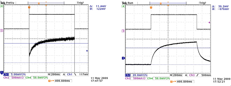
Figure 3. On-resistance of the LM3554 PFET and the ESD diode of LEDI/NETC during a flash pulse.
In steady state, the VF of the ESD diode of LEDI/NTC is -622mV, corresponding to a junction temperature of 95.2℃ (at an ambient temperature of 25℃). In steady state, the measured PFET on-resistance is 154mΩ, corresponding to a junction temperature of 105℃. Figure 3 also depicts the thermal capacitance of the LM3554. The response of VF and RPMOS shows an exponential rise similar to that of first-order RC, calculated as follows:

The heat capacity is:

The thermal capacitance obtained using the forward voltage of the ESD diode is 0.009 J/°C and the thermal capacitance obtained using the on-resistance of the PFET is 0.0044 J/°C. The difference between the temperature readings can be due to the temperature gradient across the device. The PFET is located in close proximity to the current source and is expected to heat up faster and at a higher temperature than the ESD diode at the LEDI/NTC pin, which is located further away from the power devices on the IC. The temperature difference is due to the thermal resistance and thermal capacitance between the two measurement points in the core area of the device. In addition, the response is approximately a single constant exponential. In practice, the power dissipation changes slightly as the PFET and current source heat up. This will result in a slight increase in PDISS as the junction temperature increases.
When dealing with pulsed devices such as flash LED drivers, the thermal impedance model is considered much more deeply than the thermal resistance alone. For example, the flash pulse current is 1.2A, VIN is 5V and VLED is 3.4V. In this case, the device is in power-on mode with PDISS = 2.14W. With RJ-A of 48°C/W and an ambient temperature of 50°C, the steady-state model indicates that the die temperature will rise to 153°C, which is 28°C higher than the maximum operating junction temperature. If we consider the thermal capacitance (0.0044°C/J) and factor in the 200ms flash pulse width, we can get a better estimate of the die temperature of about 113°C.
Inductor and Temperature
The discussion so far about the LM3554 and high temperatures also applies to the LM3554's power inductor. As with semiconductor devices (such as the LM3554), excessive heat dissipation in a power inductor will change the device characteristics and cause the inductor and power supply to operate abnormally. Excessive power inductor temperature usually results in increased DC winding resistance and reduced saturation current limit.
Inductor resistance
The resistance temperature coefficient of the inductor coil causes the DC resistance of the inductor to change with temperature. The coil is usually made of copper, and the temperature coefficient is about 3.9mΩ/℃. The equation for calculating its resistance is as follows:

Or equivalent to 0.39%/℃ change.
Let's look at the LM3554 again. The inductor specified in the evaluation kit is the FDSE0312-2R2 produced by Toko. At TA = 25°C, the measured resistance is 137mΩ. At 85°C, the resistance changes by 50°C × 0.39% = 19.5% (or becomes 164mΩ). At an RMS inductor current of 2A and VIN = 3.6V, the inductor resistance change causes a decrease in efficiency of about 1.5%.
Inductor Saturation
Perhaps the most concerning issue with power inductors at high temperatures is the drop in rated saturation current. When using higher RMS currents, internal power dissipation causes the inductor temperature to rise, which lowers the inductor's saturation point. At saturation, the inductor's ferromagnetic core material has reached a magnetic flux density (B(t)) that no longer increases in direct proportion to the magnetic field strength (H(t)). Instead, when at saturation, any increase in magnetic field strength due to an increase in inductor current results in a very small increase in flux density.
If we look at the switching regulator inductor current on an oscilloscope, we see that the inductor current slope increases as the device goes into saturation. This is equivalent to a decrease in inductance. The increase in ripple current will result in an increase in RMS current and switching losses in the inductor, both of which increase the power dissipation in the inductor and reduce efficiency.
Inductors can have an abrupt saturation response as they saturate at a certain point, or they can have a gradual saturation response as in the case of the FDSE0312-2R2 inductor. However, inductor manufacturers will typically specify the saturation point as a specific percentage drop in inductance value at a given current and temperature.
Figure 4 depicts an example of an inductor operating in saturation. This example uses a TDK VLS4010-2R2 (2.2μH) inductor that exhibits a sharp drop when entering saturation. The LM3554 in boost mode exhibits this effect when the minimum flash pulse width of 32ms is used. The narrow pulse width limits the self-heating of the inductor, allowing the inductor temperature to be controlled by adjusting the ambient temperature.
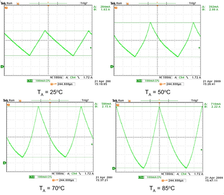
Figure 4. Inductor saturation vs. temperature.
The upper left graph of Figure 4 shows an inductor operating below the saturation point, with a normal triangular current waveform, which can be calculated by (V/L×Δt). When the peak current remains the same and the temperature rises to 50°C (upper right graph), the inductor current slope begins to increase to near the 1.76A mark, indicating that the saturation point of the inductor moves downward as the temperature rises. When the temperature rises to 70°C and then to 85°C, the entire current waveform finally appears as the inductor reaches saturation.
Estimate Inductor Temperature (Thermal Impedance)
Various factors contribute to the temperature rise of an inductor. These factors include the ambient temperature, the thermal impedance of the inductor, and the internal power dissipation of the inductor. By using the fact that the DC resistance of an inductor changes with temperature, we can estimate the operating temperature of the inductor with a relatively high accuracy. This is similar to using an ESD diode or PFET on-resistance, where the inductor coil is used as an internal thermometer.
Returning to our equation for inductor resistance versus temperature, we can calculate ΔT using the ratio of the inductor resistance at two temperatures using the following equation:
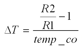
The test example shown in Figure 5 uses the VLS4010ST-2R2 in a circuit with an LM3554 with a DC current step of 1.65 A. The resistance at room temperature starts out at 65 mΩ. Over 30 seconds, the inductor reaches steady state and the resistance becomes 73 mΩ, corresponding to a steady-state operating temperature of approximately 56°C.
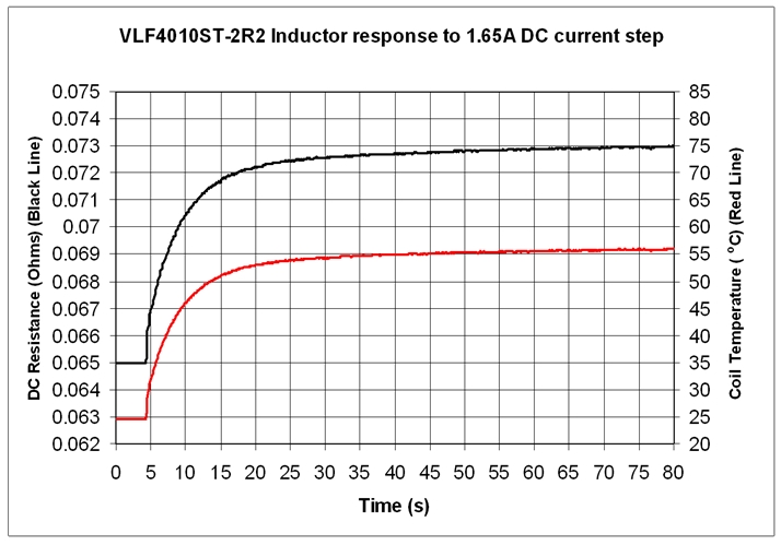
Figure 5. Inductor thermal response.
Using the definition of thermal resistance (RT), we obtain:
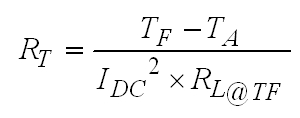
One thing to note here is that the power dissipation of an inductor is a function of its coil resistance, which changes with temperature. Therefore, it is necessary to consider calculating the TF of the inductor at a given RT. Plugging the equation for RT into the inductor resistance vs. temperature equation and solving for TF gives:

Where k is

.
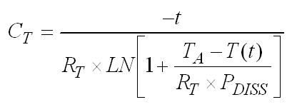
Figure 5 shows that the equivalent inductor temperature rise has approximately a first order exponential relationship with time. This again yields the equation:

The heat capacity is calculated using the following equation:
Understanding the thermal resistance of the inductor in the flash LED driver example can provide some helpful insights. Because the inductor takes a considerable amount of time to reach a stable temperature compared to the flash duration (less than 1 second), the inductor operating temperature at full flash current estimated using the steady-state thermal resistance will likely overestimate the inductor operating temperature. This can allow for a reduction in the size of an inductor operating in a pulsed device such as a flash LED driver, rather than a steady-state power supply.
Summarize
When dealing with devices that dissipate relatively large amounts of power, it is often necessary to estimate the temperature of the power management circuitry. Using generic thermal resistances is a good way to compare similar devices in the same package, but it is unlikely to yield an accurate prediction of the temperature. Therefore, it is often necessary to resort to complex thermal calculations or to directly measure the thermal resistance. This article highlights several examples that can be used to measure the temperature of a device and obtain the device's thermal resistance. Knowing the exact device temperature and the device power dissipation allows for thermal resistance calculations.
Once the thermal resistance is known, the device thermal capacitance can be calculated by taking a step change in the device power dissipation and monitoring the device temperature. This allows for a more accurate estimate of the device temperature due to transient thermal events. The examples presented in this article were done using a high current white LED flash driver, but are equally applicable to other power management devices, including those that operate in a pulsed manner and are designed to operate for long periods of time.
Previous article:Adding phosphor to UV LED to make white LED
Next article:LED lighting circuit and system level optimization analysis
Recommended ReadingLatest update time:2024-11-17 00:39


- Popular Resources
- Popular amplifiers
- MathWorks and NXP Collaborate to Launch Model-Based Design Toolbox for Battery Management Systems
- STMicroelectronics' advanced galvanically isolated gate driver STGAP3S provides flexible protection for IGBTs and SiC MOSFETs
- New diaphragm-free solid-state lithium battery technology is launched: the distance between the positive and negative electrodes is less than 0.000001 meters
- [“Source” Observe the Autumn Series] Application and testing of the next generation of semiconductor gallium oxide device photodetectors
- 采用自主设计封装,绝缘电阻显著提高!ROHM开发出更高电压xEV系统的SiC肖特基势垒二极管
- Will GaN replace SiC? PI's disruptive 1700V InnoMux2 is here to demonstrate
- From Isolation to the Third and a Half Generation: Understanding Naxinwei's Gate Driver IC in One Article
- The appeal of 48 V technology: importance, benefits and key factors in system-level applications
- Important breakthrough in recycling of used lithium-ion batteries
- Innolux's intelligent steer-by-wire solution makes cars smarter and safer
- 8051 MCU - Parity Check
- How to efficiently balance the sensitivity of tactile sensing interfaces
- What should I do if the servo motor shakes? What causes the servo motor to shake quickly?
- 【Brushless Motor】Analysis of three-phase BLDC motor and sharing of two popular development boards
- Midea Industrial Technology's subsidiaries Clou Electronics and Hekang New Energy jointly appeared at the Munich Battery Energy Storage Exhibition and Solar Energy Exhibition
- Guoxin Sichen | Application of ferroelectric memory PB85RS2MC in power battery management, with a capacity of 2M
- Analysis of common faults of frequency converter
- In a head-on competition with Qualcomm, what kind of cockpit products has Intel come up with?
- Dalian Rongke's all-vanadium liquid flow battery energy storage equipment industrialization project has entered the sprint stage before production
- Allegro MicroSystems Introduces Advanced Magnetic and Inductive Position Sensing Solutions at Electronica 2024
- Car key in the left hand, liveness detection radar in the right hand, UWB is imperative for cars!
- After a decade of rapid development, domestic CIS has entered the market
- Aegis Dagger Battery + Thor EM-i Super Hybrid, Geely New Energy has thrown out two "king bombs"
- A brief discussion on functional safety - fault, error, and failure
- In the smart car 2.0 cycle, these core industry chains are facing major opportunities!
- The United States and Japan are developing new batteries. CATL faces challenges? How should China's new energy battery industry respond?
- Murata launches high-precision 6-axis inertial sensor for automobiles
- Ford patents pre-charge alarm to help save costs and respond to emergencies
- New real-time microcontroller system from Texas Instruments enables smarter processing in automotive and industrial applications
- UPD78F0888A Renesas MCU peripheral settings
- Review summary: Kanzhi K510 CRB-KIT development kit
- ST Motor_by Changjianze1
- [Serial] [Starlight Lightning STM32F407 Development Board] Chapter 5 Buzzer Experiment
- 【ST NUCLEO-H743ZI Review】 + LIS25BA Data Collection
- 【Silicon Labs Development Kit Review 05】- Clock System Architecture
- Does this design require a separate loop for the 1 amp current?
- How to solve the problem that the leftmost work bar (Project Explorer) of CCS software disappears
- How can LM3447 achieve constant power control?
- 【Nucleo G071 Review】 Final Conclusion

 Siemens PLC Project Tutorial
 LED Cube Code
 ESP32-S3 source code


 京公网安备 11010802033920号