report presents a reference design of a 7W AC/DC LED lighting driver with TRIAC dimming. The solution uses a single-stage power factor correction (PFC) inverter topology with primary-side constant power control. The article presents a complete analysis and design of the power converter. Finally, we provide you with experimental results based on a 7W application. The design can be adapted to other applications with simple modifications.
IntroductionThis
PMP4304A reference design is a single-stage power factor correction LED driver with TRIAC dimming using the TI TPS92210 LED lighting power controller. This LED application is mainly targeted at PAR bulb replacement, which has small size, low cost, high PF and high TRIAC dimming performance.
This solution uses a single-stage power factor correction (PFC) inverter converter with primary-side constant power control. It implements primary-side constant power control in a single-stage inverter topology without an optocoupler. This driver can operate with either high-line AC or low-line AC. The output provides a constant current of 350mA to drive 6 LEDs in series.
Working Principle
2.1 Power Factor Correction Single-Stage Inverter Converter
This single-stage power factor correction converter uses an isolated inverting AC/DC topology, which rectifies the AC input line voltage into a DC output of an input sinusoidal current. The single-stage inverting topology is widely used as an isolated LED solution because it has a very low BOM cost and high efficiency.
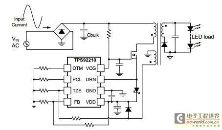
Figure 1 Single-Stage Inverter Converter
Traditional single-stage inverting solutions all use transition mode to adjust constants on time to achieve the PFC function. However, the inverting topology of transition mode is not a natural PFC because the duty cycle and frequency often change. Therefore, the accuracy of PF and THD under this condition is not high.
However, the primary side constant power single-stage inverter is a natural PFC.
First, the input voltage can be set to:
Then, the average input current can be calculated using Equation 2. Using
Equations 1 and 2, the input power is calculated as follows:

On the primary side, the constant power solution is:
In Equation 4, K is a constant, and the value of K depends on the total system power.
When the RMS of Vin changes , the duty cycle changes inversely. When the RMS of Vin is limited, the duty cycle does not change. Therefore, when the system is stable, the duty time and duty cycle are constant.
At the same time, in order to maintain constant power, the system is kept at the same switching frequency.
Since Ton , L, f, and Vin are all constants, the input current is a natural sine of Equation 2.
On the other hand, the input power is also a constant of Equation 3.
In summary, we can see that in this application, the primary side constant power single-stage scheme has certain advantages over the traditional scheme. First, the primary side constant power scheme is a natural PFC, and its PF and THD are better than the traditional scheme. Second, as the name implies, the primary side constant power scheme is only controlled by the primary side. Therefore, the optocoupler can be excluded, thereby achieving a low-cost BOM.
2.2 TPS92210 controller and system operation As for the TPS92210 controller, there is an OTM pin, which can control the Ton
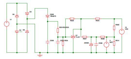
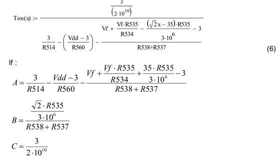
time by connecting a resistor to it ; the details are as follows: To achieve primary side constant power control, we use the following circuit, as shown in Figure 2. Figure 2 Feedforward circuit for primary-side constant power control Assuming Vin_rms = x, the relationship between Ton and Vin_rms can be calculated as follows: This formula can be simplified as Equation 7: In order to meet the requirements of primary-side constant power control (Vrms *Ton = K), select B=0. At the same time, A and C can be selected according to the input power . Figure 3 shows the simulation results after the 7W example calculation. When the input voltage becomes higher, the Ton time becomes smaller. At the same time, the input power must remain constant. Figure 3 T on time vs Vin_rms and input power vs Vin_rms 3 7W offline constant power LED lighting driver design 3.1 Design specifications Table 1 Electrical design specifications
|
Standard Project |
Minimum |
Typical Value |
Maximum |
|
Input AC voltage |
180Vac |
220Aac |
265Vac |
|
Output current tolerance |
347mA |
356mA |
372mA |
|
Number of LEDs |
6 |
||
|
Power Factor |
0.975 |
0.944 |
0.902 |
|
Efficiency without TRIAC regulation |
80.90% |
81.50% |
81.20% |
3.2 Schematic Diagram

Figure 4 PMP4304A schematic diagram
3.3 PCB Layout 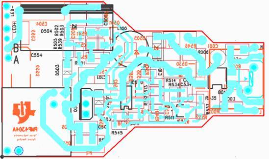
Figure 5 Board Assembly Diagram - Layer 1 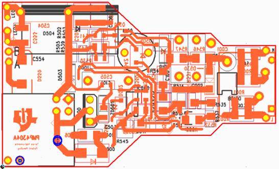
Figure 6 Board Assembly Diagram - Layer 2
3.4 Efficiency 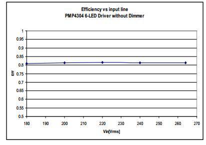
Figure 7 Efficiency vs. Input Voltage
3.5 Line Regulation 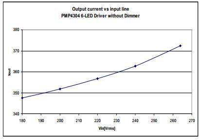
Figure 8 Output Current vs. Input Voltage
3.6 Power Factor 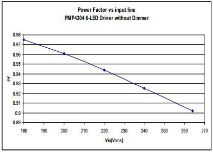
Figure 9 Power Factor vs. Input Voltage
3.7 TRIAC Dimming Performance
Table 2 Output Current at Different Dimming Controller Conduction Angles 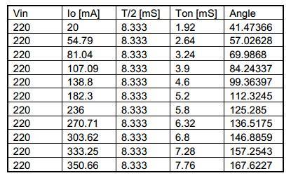
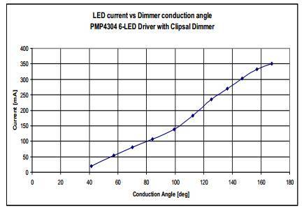
Figure 10 Output Current vs. Dimming Controller Conduction Angles 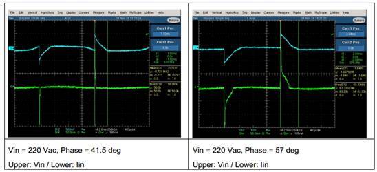
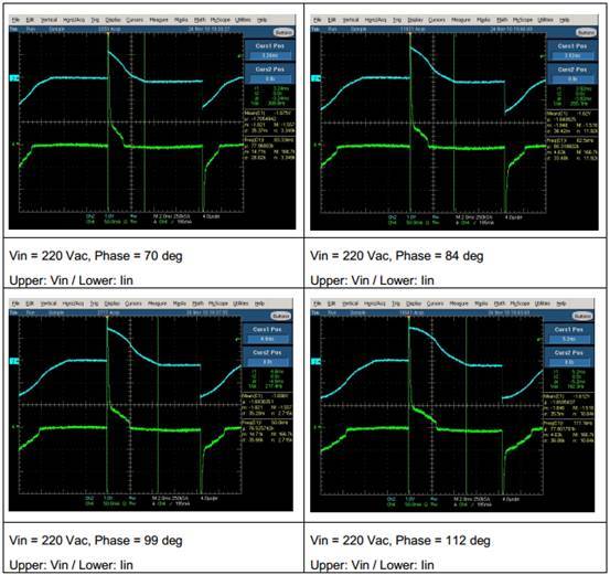
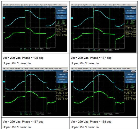
Figure 11 Input Current vs. Input Voltage at Different Conduction Angles
4 Conclusion
This paper analyzes the primary-side constant power control single-stage inverting LED driver and introduces the advantages of using primary-side control based on TPS92210. At the same time, we also implemented a real 7W design. It shows many benefits of the TPS92210 solution, such as small size, low cost, high PF, and high TRIAC dimming performance.
References
1, "TPS92210 Product Manual", LED Lighting Power Controller
Previous article:Multisim 10-LED is more colorful! Design and simulation of color control transformation
Next article:6W LED Driver PI LYT0006P Review
- Popular Resources
- Popular amplifiers
- MathWorks and NXP Collaborate to Launch Model-Based Design Toolbox for Battery Management Systems
- STMicroelectronics' advanced galvanically isolated gate driver STGAP3S provides flexible protection for IGBTs and SiC MOSFETs
- New diaphragm-free solid-state lithium battery technology is launched: the distance between the positive and negative electrodes is less than 0.000001 meters
- [“Source” Observe the Autumn Series] Application and testing of the next generation of semiconductor gallium oxide device photodetectors
- 采用自主设计封装,绝缘电阻显著提高!ROHM开发出更高电压xEV系统的SiC肖特基势垒二极管
- Will GaN replace SiC? PI's disruptive 1700V InnoMux2 is here to demonstrate
- From Isolation to the Third and a Half Generation: Understanding Naxinwei's Gate Driver IC in One Article
- The appeal of 48 V technology: importance, benefits and key factors in system-level applications
- Important breakthrough in recycling of used lithium-ion batteries
- LED chemical incompatibility test to see which chemicals LEDs can be used with
- Application of ARM9 hardware coprocessor on WinCE embedded motherboard
- What are the key points for selecting rotor flowmeter?
- LM317 high power charger circuit
- A brief analysis of Embest's application and development of embedded medical devices
- Single-phase RC protection circuit
- stm32 PVD programmable voltage monitor
- Introduction and measurement of edge trigger and level trigger of 51 single chip microcomputer
- Improved design of Linux system software shell protection technology
- What to do if the ABB robot protection device stops
- Huawei's Strategic Department Director Gai Gang: The cumulative installed base of open source Euler operating system exceeds 10 million sets
- Download from the Internet--ARM Getting Started Notes
- Learn ARM development(22)
- Learn ARM development(21)
- Learn ARM development(20)
- Learn ARM development(19)
- Learn ARM development(14)
- Learn ARM development(15)
- Analysis of the application of several common contact parts in high-voltage connectors of new energy vehicles
- Wiring harness durability test and contact voltage drop test method
- [MSP430F5529 Review] 7. TFT Color Screen Snake
- TI C2000 Basic Learning
- Interest group training topic: Use MOS tube or + op amp to realize a DC/DC closed-loop voltage regulator
- Simple square wave generator based on 51 single chip microcomputer
- MSP430fr6989 serial port DMA sending experimental routine
- [RISC-V MCU CH32V103 Review] First impression of CH32V103C8T6 chip
- 100 check items for PCB design to ensure you have no problems with your design!
- How to write the corresponding program process according to the timing diagram
- Differences and similarities between detection circuits, filter circuits, frequency selection circuits, threshold comparison circuits, and bandpass circuits
- When designing PCB, how to consider electromagnetic compatibility EMC/EMI, specifically...

 TLV2252AQD


 京公网安备 11010802033920号