LEDs are an attractive light source due to their high reliability (lifetime of over 50,000 hours), high efficiency (>120 lumens/watt), and near-instantaneous response time. LEDs emit light in just 5nS, compared to the 200mS response time of an incandescent bulb. As a result, they are now widely used in brake lights in the automotive industry.
Driving LEDs
Driving LEDs is not without its challenges. Adjustable brightness requires driving the LED with a constant current, and that current must remain constant regardless of the input voltage. This is more challenging than simply connecting an incandescent bulb to a battery to power it.
LEDs have a forward VI characteristic similar to that of a diode. Below the LED turn-on threshold (about 3.5V for white LEDs), the current through the LED is very small. Above this threshold, the current increases exponentially as a function of the forward voltage. This allows the LED to be modeled as a voltage source with a series resistor, with a caveat: this model is only valid for a single operating DC current. If the DC current in the LED changes, the model's resistors should also change to reflect the new operating current. At large forward currents, the power dissipated in the LED causes the device to heat up, which changes the forward voltage drop and dynamic impedance. It is important to consider the thermal environment when determining the LED impedance.
When driving an LED through a buck regulator, the LED often conducts the inductor's AC ripple current and the DC current, depending on the output filter arrangement chosen. This not only increases the RMS amplitude of the current in the LED, but also increases its power dissipation. This increases the junction temperature and has a significant impact on the LED's lifetime. If we set a 70% light output limit as the LED's lifetime, the LED's lifetime will increase from 15,000 hours at 74 degrees Celsius to 40,000 hours at 63 degrees Celsius. The power loss of the LED is determined by the LED resistance times the square of the RMS current plus the average current times the forward voltage drop. Since the junction temperature is determined by the average power dissipation, even larger ripple currents have little effect on the power dissipation. For example, in a buck converter, a peak-to-peak ripple current equal to the DC output current (Ipk-pk = Iout) will increase the total power loss by no more than 10%. If the above loss levels are exceeded, the AC ripple current from the power supply needs to be reduced to keep the junction temperature and operating life constant. A very useful rule of thumb is that for every 10 degrees Celsius reduction in junction temperature, the semiconductor life will increase by a factor of two. In practice, most designs tend to go for lower ripple currents due to the damping effect of the inductor. In addition, the peak current in the LED should not exceed the maximum safe operating current rating specified by the manufacturer.
Analysis on topological structure selection of LED drive power supply
In LED lighting applications using AC-DC power supplies, the building blocks of power conversion include discrete components such as diodes, switches (FETs), inductors, capacitors, and resistors to perform their respective functions, while pulse width modulation (PWM) regulators are used to control power conversion. Isolated AC-DC power conversion, which usually incorporates a transformer in the circuit, includes flyback, forward, and half-bridge topologies, as shown in Figure 3, where the flyback topology is the standard choice for low- to medium-power applications with power less than 30 W, while the half-bridge structure is most suitable for providing higher energy efficiency/power density. As for the transformer in the isolation structure, its size is related to the switching frequency, and most isolated LED drivers basically use "electronic" transformers.
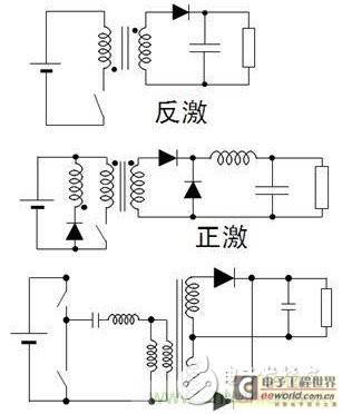
Figure 1: LLC half-bridge resonant topology
In LED lighting applications using DC-DC power supplies, the LED drive methods that can be used include resistor type, linear regulator and switching regulator. The basic application diagram is shown in Figure 4. In the resistor type drive method, the forward current of the LED can be controlled by adjusting the current detection resistor in series with the LED. This drive method is easy to design, low cost, and has no electromagnetic compatibility (EMC) problems. The disadvantages are that it depends on voltage, requires binning of LEDs, and has low energy efficiency. Linear regulators are also easy to design and have no EMC problems. They also support current stabilization and overcurrent protection (fold back) and provide external current set points. The disadvantages are power dissipation problems, the input voltage must always be higher than the forward voltage, and the energy efficiency is not high. The switching regulator continuously controls the on and off of the switch (FET) through the PWM control module, thereby controlling the flow of current.

Figure 2: Common DC-DC LED drive methods
Switching regulators have higher energy efficiency, are independent of voltage, and can control brightness. However, their disadvantages are relatively high cost, higher complexity, and electromagnetic interference (EMI) issues. Common topologies of LED DC-DC switching regulators include different types such as buck, boost, buck-boost, or single-ended primary inductor converter (SEPIC). Among them, the buck structure is used when the minimum input voltage under all working conditions is greater than the maximum voltage of the LED string, such as using 24 Vdc to drive 6 LEDs in series; on the contrary, the boost structure is used when the maximum input voltage under all working conditions is less than the minimum output voltage, such as using 12 Vdc to drive 6 LEDs in series; and when the input voltage and output voltage range overlap, the buck-boost or SEPIC structure can be used, such as using 12 Vdc or 12 Vac to drive 4 LEDs in series, but the cost and energy efficiency of this structure are the least ideal.
The method of using AC power to directly drive LEDs has also gained some development in recent years. See Figure 5 for its application diagram. In this structure, the LED strings are arranged in opposite directions, working in half cycles, and the LEDs are turned on only when the line voltage is greater than the forward voltage. This structure has its advantages, such as avoiding power losses caused by AC-DC conversion. However, in this structure, the LEDs are switched at a low frequency, so the human eye may perceive flickering. In addition, LED protection measures need to be added in this design to protect them from line surges or transients.
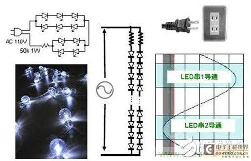
Figure 3: Schematic diagram of driving LEDs directly using AC LED topology selection example analysis
The information shown in Figure 4 helps you choose the best switching topology for your LED driver. In addition to these topologies, you can use simple current limiting resistors or linear regulators to drive the LEDs, but these methods usually waste too much power. All relevant design parameters include input voltage range, number of LEDs driven, LED current, isolation, EMI suppression, and efficiency. Most LED driver circuits belong to the following topology types: buck, boost, buck-boost, SEPIC, and flyback.
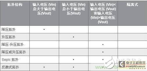
Figure 4: Alternative LED power supply topologies
Figure 5 shows three basic examples of power topologies. The first schematic shows a buck regulator that is suitable for situations where the output voltage is always less than the input voltage. In Figure 5, the buck regulator controls the current into the LED by varying the on-time of the MOSFET. Current sensing is achieved by measuring the voltage across a resistor that should be in series with the LED. The important design challenge for this approach is how to drive the MOSFET. From a cost-effective perspective, it is recommended to use an N-channel field effect transistor (FET) that requires a floating gate drive. This requires a drive transformer or a floating drive circuit that can be used to maintain an internal voltage higher than the input voltage.
Figure 5 also shows an alternative step-down regulator (buck #2). In this circuit, the MOSFET drives ground, greatly reducing the drive circuit requirements. The circuit has the option of sensing the LED current by monitoring the FET current or a current-sense resistor in series with the LED. The latter requires a level-shifting circuit to obtain information about the power supply ground, but this complicates a simple design. Figure 5 also shows a boost converter that can be used when the output voltage is always greater than the input voltage. This topology is easy to design because the MOSFET drives ground and the current-sense resistor is also ground-referenced. One drawback of this circuit is that during a short circuit, the current through the inductor is unlimited. You can add fault protection in the form of fuses or electronic circuit breakers. In addition, some more complex topologies can also provide such protection.

Figure 5: Simple buck and boost topologies for powering LEDs
Figure 6 shows two buck-boost circuits that can be used when the input voltage is higher or lower than the output voltage. Both have the same trade-off characteristics (the trade-offs are shown in the two buck topologies regarding the location of the current sense resistor and the gate drive). The buck-boost topology in Figure 6 shows a ground referenced gate drive. It requires a level shifted current sense signal, but the inverting buck-boost circuit has a ground referenced current sense and level shifted gate drive. If the control IC is associated with the negative output, and the current sense resistor and LED are swapped, then the inverting buck-boost circuit can be configured in a very useful way. With the appropriate control IC, the output current can be measured directly, and the MOSFET can be driven directly.
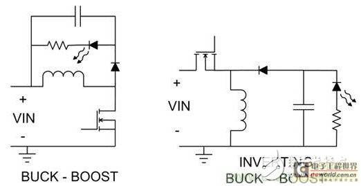
Figure 6: The buck-boost topology can regulate input voltages greater or less than Vout.
One drawback of the buck-boost approach is that the currents are quite high. For example, when the input and output voltages are the same, the inductor and power switch currents are twice the output current. This can negatively impact efficiency and power consumption. In many cases, the “buck or boost” topology in Figure 7 will alleviate these issues. In this circuit, a buck power stage is followed by a boost. If the input voltage is higher than the output voltage, the buck stage regulates while the boost stage is just powered on. If the input voltage is less than the output voltage, the boost stage regulates while the buck stage is powered on. Some overlap is usually allowed for the boost and buck operation, so there is no deadband when going from one model to the other.
The benefit of this circuit is that the switch and inductor currents are nearly equal to the output current when the input and output voltages are nearly equal. The inductor ripple current also tends to be smaller. Even though there are four power switches in this circuit, efficiency is usually significantly improved, which is critical in battery applications. The SEPIC topology is also shown in Figure 7, which requires fewer FETs but more passive components. The benefit is a simple ground-referenced FET driver and control circuit. In addition, the dual inductors can be combined into a single coupled inductor, saving space and cost. But like the buck-boost topology, it has higher switch currents than the "buck or boost" and pulsating output currents, which requires capacitors that can carry larger RMS currents.

Figure 7: Buck or boost and SEPIC topologies offer higher efficiency
Safety considerations may dictate the use of isolation between the offline voltage and the output voltage. In this application, the most cost-effective solution is the flyback converter (see Figure 8). It requires the lowest number of components of all the isolation topologies. The transformer turns ratio can be designed for buck, boost, or buck-boost output voltages, which provides great design flexibility. However, the disadvantage is that the power transformer is usually a custom component. In addition, there is high component stress in the FETs and input and output capacitors. In steady-state lighting applications, the power factor correction (PFC) function can be implemented by using a "slow" feedback control loop that regulates the LED current in phase with the input voltage. A high power factor is achieved by regulating the desired average LED current and the input current in phase with the input voltage.
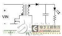
Figure 8: A flyback converter provides both isolation and power factor correction
Dimming Technology
It is not uncommon to need to dim LEDs. For example, you may need to dim a display or adjust the brightness of an architectural light. There are two ways to do this: either reduce the LED current or turn the LED on and off quickly and then let the eye eventually balance. Because light output is not completely linear with current, reducing current is the least efficient method. In addition, the LED color spectrum usually changes at currents below the rated value. Remember that human perception of brightness is exponential, so dimming requires a larger percentage change in current. This has a significant impact on circuit design because a 3% regulation error at full current can magnify into a 30% or more error at 10% load due to circuit tolerances. Although there are response speed issues, regulating current through pulse width modulation (PWM) is still more precise. When lighting and display, PWM above 100Hz is required to make the human eye not notice the flicker. The 10% pulse width is in the millisecond range and requires a power supply with a bandwidth of more than 10 kHz.
in conclusion
As shown in Figure 9, the use of LEDs in many applications is becoming increasingly common. It will use a variety of power supply topologies to support these applications. Generally, the input voltage, output voltage and isolation requirements will dictate the correct choice. When the input voltage is always higher or lower than the output voltage, using a buck or boost may be the obvious choice. However, when the relationship between the input and output voltages is not so constrained, the choice becomes more difficult and requires weighing many factors, including efficiency, cost and reliability.

Figure 9: Many LED applications specify multiple power supply topologies
Previous article:A brief discussion on the selection techniques of driver chips for LED lighting
Next article:Comprehensive interpretation of LED lamp characteristics and standards
Recommended ReadingLatest update time:2024-11-17 02:27

- Popular Resources
- Popular amplifiers
- MathWorks and NXP Collaborate to Launch Model-Based Design Toolbox for Battery Management Systems
- STMicroelectronics' advanced galvanically isolated gate driver STGAP3S provides flexible protection for IGBTs and SiC MOSFETs
- New diaphragm-free solid-state lithium battery technology is launched: the distance between the positive and negative electrodes is less than 0.000001 meters
- [“Source” Observe the Autumn Series] Application and testing of the next generation of semiconductor gallium oxide device photodetectors
- 采用自主设计封装,绝缘电阻显著提高!ROHM开发出更高电压xEV系统的SiC肖特基势垒二极管
- Will GaN replace SiC? PI's disruptive 1700V InnoMux2 is here to demonstrate
- From Isolation to the Third and a Half Generation: Understanding Naxinwei's Gate Driver IC in One Article
- The appeal of 48 V technology: importance, benefits and key factors in system-level applications
- Important breakthrough in recycling of used lithium-ion batteries
- Innolux's intelligent steer-by-wire solution makes cars smarter and safer
- 8051 MCU - Parity Check
- How to efficiently balance the sensitivity of tactile sensing interfaces
- What should I do if the servo motor shakes? What causes the servo motor to shake quickly?
- 【Brushless Motor】Analysis of three-phase BLDC motor and sharing of two popular development boards
- Midea Industrial Technology's subsidiaries Clou Electronics and Hekang New Energy jointly appeared at the Munich Battery Energy Storage Exhibition and Solar Energy Exhibition
- Guoxin Sichen | Application of ferroelectric memory PB85RS2MC in power battery management, with a capacity of 2M
- Analysis of common faults of frequency converter
- In a head-on competition with Qualcomm, what kind of cockpit products has Intel come up with?
- Dalian Rongke's all-vanadium liquid flow battery energy storage equipment industrialization project has entered the sprint stage before production
- Allegro MicroSystems Introduces Advanced Magnetic and Inductive Position Sensing Solutions at Electronica 2024
- Car key in the left hand, liveness detection radar in the right hand, UWB is imperative for cars!
- After a decade of rapid development, domestic CIS has entered the market
- Aegis Dagger Battery + Thor EM-i Super Hybrid, Geely New Energy has thrown out two "king bombs"
- A brief discussion on functional safety - fault, error, and failure
- In the smart car 2.0 cycle, these core industry chains are facing major opportunities!
- Rambus Launches Industry's First HBM 4 Controller IP: What Are the Technical Details Behind It?
- The United States and Japan are developing new batteries. CATL faces challenges? How should China's new energy battery industry respond?
- Murata launches high-precision 6-axis inertial sensor for automobiles
- Ford patents pre-charge alarm to help save costs and respond to emergencies
- 【XMC4800 Relax EtherCAT Kit Review】+ Getting started with DAVE, RTC module applications and issues
- DSP suddenly freezes while the program is running
- Can you tell what is different about 5G?
- [Open Source] Development Board Power-On Tutorial - Crazy Shell Development Board Series
- Problems with freewheeling diodes in MOS drive motors
- How to solve the problem of abnormal heating of op amp THS4052ID
- [Home Smart Lighting Control and Indoor Environment Monitoring System]--5. [RSL10] Bluetooth BLE Host Computer Development 1
- Antenna-on-Package Design Simplifies mmWave Sensing in Buildings and Factories
- Getting Started with MPlab Programming for PIC16F1823
- LDO Basics: Noise - Part 2

 Siemens PLC Project Tutorial
 LED Cube Code
 ESP32-S3 source code


 京公网安备 11010802033920号