introduction
The LCD screen itself does not emit light. In order to clearly see the content of the LED display, a certain amount of white light backlight is required. The backlight is an optical component inside the LCD display, which is composed of a light source and necessary optical auxiliary components. If the LED backlight is increased by contrast, regional control and other means, the performance is far better than the CCFL backlight. At present, LED backlights have been popularized in small and medium-sized panels, such as mobile phones, digital photo frames, etc. With the development of LED technology and the continuous maturity of LED chips, LED LCD TVs may gradually replace traditional CCFL LCD TVs.
Backlight sources are divided into direct-lit backlight sources and edge-lit backlight sources according to the position of the light source. In direct-lit backlight sources, the LED light source is placed directly below the light-emitting surface. The light emitted by the light source is diffused and mixed by the diffusion plate over a certain distance and then emitted as a surface light source. Direct-lit backlight sources require a certain light mixing distance. The edge-lit backlight structure is more advantageous for ultra-thin module design. With the rise of the "ultra-thin trend", large-size ultra-thin edge-lit LED backlight sources have become a research hotspot for major TV manufacturers and upstream companies.
1 Structural design
The LED backlight designed in this paper is an ultra-thin side-lit structure. The entire structure includes: LED light strip, driver board, film material, light guide plate, heat sink, upper frame, and backboard. The backlight uses white light LED. The entire structural design takes the center point of the Active Area as the design center of all components, and designs other dimensions based on the size of the LCD screen used in LCD TVs. The structure is designed by comprehensively considering the requirements of circuit design and optical design. The structural design starts with the UⅣOUT layout diagram to express the overall mechanism and the assembly relationship between each component, and then proceeds to the parts drawing structure design. The upper frame adopts a segmented design, which is segmented in the length direction to avoid excessive length. The outlet ends of the light strip are set at the four corners of the backboard to reduce the winding length.
2 Optical Design
The function of the backlight module is to transform the light emitted by a point light source into a surface light source through diffuse reflection. In order to obtain a qualified surface light source, the first thing to do is to select a suitable LED. This design uses a white light dual-chip LED. By presetting the white field photometric index and combining the research and analysis of influencing factors such as the LCD screen and optical film, the calculation of the luminous flux required for the entire backlight source is completed. Based on the calculated luminous flux, combined with the optical characteristics of the LED, the number of LEDs required is calculated. Table 1 shows the electrical and optical characteristics of the selected LEDs.
Table 1 LED electrical and optical properties

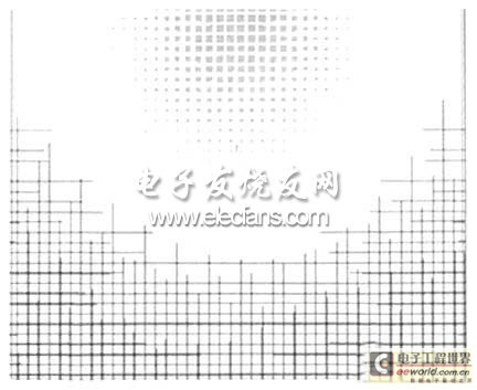
In order to improve the brightness of the backlight source, the film material structure is matched as follows: a layer of diffuser + a layer of BEF + a layer of DBEF. Among them, the role of the diffuser is to atomize the light by refraction and reflection of the diffuser material, so that the emitted light is more uniform: the role of BEF is to gather the light so that it enters the liquid crystal module vertically to increase the brightness: DBEF uses 50% of the light originally absorbed by the traditional absorption polarizer to increase the brightness. The diameter of the light guide plate mesh point is 0.54~1.55mm. Figure 1 shows the distribution diagram of some mesh points of the light guide plate.

Figure 1 Light guide plate dot distribution diagram
3 Circuit Design
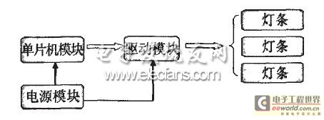
The LED backlight circuit design mainly includes the light bar design and the drive control circuit design. Figure 2 shows the structural block diagram of the entire circuit part.

Figure 2 Circuit structure diagram
3.1 Light bar design
The light source uses a dual-chip white light LED, and the light strips are distributed around the backlight source. In order to achieve better current uniformity, the light strips are connected in series and parallel, and two parallels are connected in multiple strings. In order to achieve better heat dissipation, the LED light strips are made of aluminum substrate. The input voltage of the entire system is 24V, which is provided by an external power converter.
3.2 Drive control circuit design
The driver chip is a three-way peak current mode PWM controller that provides high-precision LED current by closed-loop control of the output current. The chip contains three peak current mode controllers that provide feedback to the IC to ensure higher efficiency and higher accuracy. The gate driver on the chip is optimized to drive a logic-level FET with a source current of 0.25A or a sink current of 0.5A, and each output current can be dimmed individually by linear or PWM dimming methods.
The closed-loop system of the chip can dynamically adjust its output voltage to adapt to the line and load adjustment of the LED current. The three-way driver integrated in a single package ensures better current matching between each string, while reducing the number of chips in the entire system. It has a 40V linear regulator to provide 5V power to power the IC. The switching frequency of the three converters is controlled by an internal oscillator, and the three channels have a phase difference of 1200 to reduce input current ripple. High-voltage drive, good current matching. The current accuracy between LED strings is 4-2%, and linear and PWM dimming are supported.

Figure 3 PW_M_ waveform
3.3 Heat dissipation design
Since LED has low light efficiency, it will generate a lot of heat when working. If the heat dissipation problem is not solved, the brightness of LED will be attenuated and the service life will be shortened. In order to suppress the heat generated by LED from affecting the brightness and color of the backlight module, it is necessary to carry out heat dissipation design for LED.
In order to achieve better heat dissipation, the LED array is welded on an aluminum substrate (MCPCB), which has many times better heat dissipation effect than ordinary PCB (FR4 material PCB). Under the aluminum substrate, a long strip heat sink is designed. A heat-conducting double-sided adhesive is applied between the heat sink and the light bar, and the aluminum substrate and the heat sink are fixed with screws. A heat-conducting sheet with a protective film is applied to the heat accumulation area around the backlight source. In order to reduce thermal resistance, thermal vias are added to the LED pad. In this way, the cross-sectional area of the PCB board perpendicular to the heat flow direction is reduced, thereby reducing the thermal resistance between the top and bottom layers and enhancing the heat conduction of the LED lamp. Finally, the heat is dissipated by air convection in the TV case.
4 Test Results
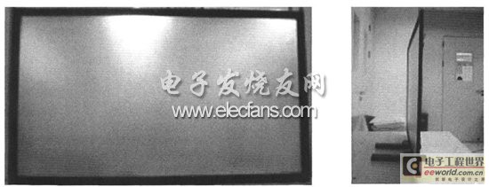
The ultra-thin LED backlight for LCD TV designed in this paper is a side-lit structure, and the light source uses white LED. Figure 4 shows the assembled LED backlight, which is 9.9mm thick. The nine-point test using BM-7 showed a central brightness of 5,500nit, a brightness uniformity of 82%, and a color reproduction of 95%@CIE 1976. The overall power of the backlight is 150W, of which the LED power consumption is 135W, and the drive circuit efficiency is 90%. The drive circuit of the backlight system is a high-voltage drive with a simple circuit and good current consistency.

Figure 4 Assembled backlight source
5 Conclusion
This paper designs a large-size ultra-thin LED backlight for LCD TVs, with a center brightness of 5,500nit, an overall backlight power of 150W, and a brightness uniformity of 82%. The thickness of the whole machine is 9.9mm, reaching the industry-leading level. The backlight designed in this paper has passed the reliability test, laying the foundation for mass production.
Previous article:Introduction to the working principle of LED display technology
Next article:Analysis of LED application in backlight module
Recommended ReadingLatest update time:2024-11-16 23:33


- Popular Resources
- Popular amplifiers
- MathWorks and NXP Collaborate to Launch Model-Based Design Toolbox for Battery Management Systems
- STMicroelectronics' advanced galvanically isolated gate driver STGAP3S provides flexible protection for IGBTs and SiC MOSFETs
- New diaphragm-free solid-state lithium battery technology is launched: the distance between the positive and negative electrodes is less than 0.000001 meters
- [“Source” Observe the Autumn Series] Application and testing of the next generation of semiconductor gallium oxide device photodetectors
- 采用自主设计封装,绝缘电阻显著提高!ROHM开发出更高电压xEV系统的SiC肖特基势垒二极管
- Will GaN replace SiC? PI's disruptive 1700V InnoMux2 is here to demonstrate
- From Isolation to the Third and a Half Generation: Understanding Naxinwei's Gate Driver IC in One Article
- The appeal of 48 V technology: importance, benefits and key factors in system-level applications
- Important breakthrough in recycling of used lithium-ion batteries
- Innolux's intelligent steer-by-wire solution makes cars smarter and safer
- 8051 MCU - Parity Check
- How to efficiently balance the sensitivity of tactile sensing interfaces
- What should I do if the servo motor shakes? What causes the servo motor to shake quickly?
- 【Brushless Motor】Analysis of three-phase BLDC motor and sharing of two popular development boards
- Midea Industrial Technology's subsidiaries Clou Electronics and Hekang New Energy jointly appeared at the Munich Battery Energy Storage Exhibition and Solar Energy Exhibition
- Guoxin Sichen | Application of ferroelectric memory PB85RS2MC in power battery management, with a capacity of 2M
- Analysis of common faults of frequency converter
- In a head-on competition with Qualcomm, what kind of cockpit products has Intel come up with?
- Dalian Rongke's all-vanadium liquid flow battery energy storage equipment industrialization project has entered the sprint stage before production
- Allegro MicroSystems Introduces Advanced Magnetic and Inductive Position Sensing Solutions at Electronica 2024
- Car key in the left hand, liveness detection radar in the right hand, UWB is imperative for cars!
- After a decade of rapid development, domestic CIS has entered the market
- Aegis Dagger Battery + Thor EM-i Super Hybrid, Geely New Energy has thrown out two "king bombs"
- A brief discussion on functional safety - fault, error, and failure
- In the smart car 2.0 cycle, these core industry chains are facing major opportunities!
- The United States and Japan are developing new batteries. CATL faces challenges? How should China's new energy battery industry respond?
- Murata launches high-precision 6-axis inertial sensor for automobiles
- Ford patents pre-charge alarm to help save costs and respond to emergencies
- New real-time microcontroller system from Texas Instruments enables smarter processing in automotive and industrial applications
- Designing efficient, powerful, and fast electric vehicle charging stations
- 《GitHub Introduction and Practice》
- A new generation of linear and efficient base station power amplifier technology
- I would like to ask how to calculate the gain of the PCB antenna
- Multi-channel RF transceiver clocking for radar and wireless 5G testers
- CC2541 cannot receive data sent by Bluetooth main module
- Several analysis methods that you must know about transistor circuits!
- [GD32L233C] + 5. Use RTThread's Finsh component
- Please design a pressure sensor conversion circuit
- Do you know these three special PCB routing techniques?

 Siemens PLC Project Tutorial
 LED Cube Code
 ESP32-S3 source code


 京公网安备 11010802033920号