Multi-core architecture opens up new directions in performance improvement and energy-saving computing. The connection method between cores and the communication coordination method are all research focuses. The research of this topic is based on the handheld spectrum analyzer system platform, which adopts the three-core architecture of ARM, DSP, and FPGA. Each core completes different tasks, and then the cores send parameters and exchange data to realize the system functions. The design focus is to solve the communication problem between cores.
1 Hardware Design of Communication between ARM, DSP and FPGA
The intermediate frequency signal processing board of the handheld spectrum analyzer mainly includes four parts: analog-to-digital converter (AD9244), FPGA (XS3C5000), DSP (TMS320C6412), and ARM (AT91RM9200). The position and function of ARM in the handheld spectrum analyzer are shown in Figure 1.

The hardware design of ARM refers to the evaluation board data provided by Atmel. It mainly includes the design of the following unit circuits: power supply circuit, clock circuit, reset circuit, startup mode selection circuit, JTAG interface circuit, Debug serial port circuit, external expansion SDRAM circuit, external expansion NOR Flash (AM29LV320DB) circuit, HPI interface circuit for communication with DSP, SPI interface circuit for communication with FPGA, I2C interface circuit for connecting temperature sensor, and Ethernet interface circuit.
1.1 HPI interface circuit design
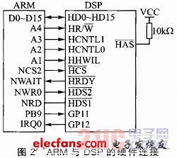
The HPI bus of ARM and DSP uses 16-bit data communication, and the HPI bus multiplexes data and addresses. ARM uses some address signal lines to connect to the HPI bus control signal of DSP, and controls the HPI bus by changing the address. The hardware connection between ARM and DSP is shown in Figure 2. Among them, ARM selects to operate on the HPI C, HPIA, and HPID registers through the connection of address lines A3 and A2 with the HCNTL1 and HCNTL0 pins of DSP. The half-word selection when reading and writing is performed by connecting A1 with the HHWIL pin of DSP. The reading and writing is selected by connecting A4 with the pin. ARM sends a handshake signal to the GP11 pin of DSP through PB9, and DSP interrupts ARM through the GP12 pin to start data transmission.

1.2 SPI interface circuit design
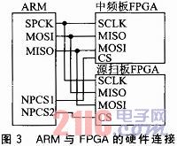
The SPI interface is a serial communication interface, which consists of 4 signal lines, among which SPCK, MOSI, and MISO are multiplexed. ARM uses the chip select signal NPCS to select communication with different slave devices. In this project, ARM communicates with the IF board FPGA and the source scan board FPGA respectively through the SPI bus. The hardware connection between ARM and FPGA is shown in Figure 3. ARM is in host mode, and its SPI interface's SPCK, MISO, and MOSI are connected to the slave FPGA's SCLK, MOSI, and MISO respectively. ARM has a total of 4 chip select lines. Here, NPCS1 is used to select the IF board FPGA, and NPCS2 is used to select the source scan board FPGA.

2 Communication Mechanism between Multi-cores
2.1 Communication mechanism between ARM and DSP
After the Linux system is started, ARM will first perform a series of initializations, including initialization of communication interfaces such as HPI and SPI and restarting DSP to achieve timing synchronization. After the initialization is completed, ARM will send a handshake signal to DSP, that is, write data to the GP11 port of DSP through PB9, indicating that ARM has completed initialization and can receive data sent by DSP. After the DSP completes data processing, it will wait for the handshake signal from ARM, that is, it will continuously access the GP11 port to see if it has received data. When the DSP receives the handshake signal, it will write 1 to the GP12 port to interrupt other work of the ARM host so that ARM can read the data processed by DSP. After receiving the interrupt signal, ARM clears the interrupt by setting HCNTL0 and HCNTL1 to operate HPIC, and then writes HPIA to tell DSP where to start self-increment reading. Then DSP transfers data from DMA to HPID, and ARM obtains data by reading HPID. Since the HPI interface between ARM and DSP is 16-bit data transmission, the software needs to realize the merging of the 16-bit data read twice into 32 bits, and then pass it to the upper-level application. After ARM finishes reading the data, it writes 0xffffffff to the specified address of DSP to notify DSP that the read is successful and to prepare for the next data transmission.
After receiving the command from the upper application, ARM obtains various parameters by parsing and calculating the command. Then it sends it to DSP through HPI. The process is: first write HPIC register through HCNT L0 and HCNTL1 to configure the read-write mode. Then write HPIA register to set the physical address of writing to DSP. Send control parameters by continuously writing HPID register, and finally write 0x5555aaaa to indicate that the sending is completed.
2.2 Communication mechanism between ARM and FPGA
ARM integrates the SPI interface and communicates data with FPGA through SPI. The "single master and multiple slaves" mode of the SPI bus is just suitable for the communication between ARM and the IF board FPGA and the source scan board FPG A in this project. After ARM starts the Linux system, it first initializes the SPI interface, including programming the PIO controller, assigning SPI pins to peripherals, configuring the PMC (power management controller) to enable the SPI clock, and configuring ARM to host mode. When the upper-layer software sends a command, ARM first parses the received command word and parses the command to obtain various parameters: after calculation, the SPI interface chip select NPCS is used to select the IF board FPGA or the source scan board FPGA to send the parameters.
Since the functions of the IF board FPGA and the source scan board FPGA are different and the received parameters are also different, different data frame formats and transmission rules are formulated. ARM transmits 16 bits per frame of data to the IF board FPGA, and the transmission frequency is 0.36 MHz. The transmission order is: routing code 1, data frame 1, routing code 2, data frame 2, end code. ARM transmits 16 bits per frame of data to the source scan board FPGA, and the transmission frequency is 0.36 MHz. Before sending a parameter, a virtual address that stores the parameter must be sent first, and then the parameter is sent, in the order of: virtual address 1, parameter 1, virtual address 2, parameter 2, end code.
Previous article:What is the difference between a spectrum analyzer and an oscilloscope?
Next article:Technical Articles—How Infrared Thermal Imaging Detects Your Body Temperature
- New IsoVu™ Isolated Current Probes: Bringing a New Dimension to Current Measurements
- Modern manufacturing strategies drive continuous improvement in ICT online testing
- Methods for Correlation of Contact and Non-Contact Measurements
- Keysight Technologies Helps Samsung Electronics Successfully Validate FiRa® 2.0 Safe Distance Measurement Test Case
- From probes to power supplies, Tektronix is leading the way in comprehensive innovation in power electronics testing
- Seizing the Opportunities in the Chinese Application Market: NI's Challenges and Answers
- Tektronix Launches Breakthrough Power Measurement Tools to Accelerate Innovation as Global Electrification Accelerates
- Not all oscilloscopes are created equal: Why ADCs and low noise floor matter
- Enable TekHSI high-speed interface function to accelerate the remote transmission of waveform data
- Intel promotes AI with multi-dimensional efforts in technology, application, and ecology
- ChinaJoy Qualcomm Snapdragon Theme Pavilion takes you to experience the new changes in digital entertainment in the 5G era
- Infineon's latest generation IGBT technology platform enables precise control of speed and position
- Two test methods for LED lighting life
- Don't Let Lightning Induced Surges Scare You
- Application of brushless motor controller ML4425/4426
- Easy identification of LED power supply quality
- World's first integrated photovoltaic solar system completed in Israel
- Sliding window mean filter for avr microcontroller AD conversion
- What does call mean in the detailed explanation of ABB robot programming instructions?
- STMicroelectronics discloses its 2027-2028 financial model and path to achieve its 2030 goals
- 2024 China Automotive Charging and Battery Swapping Ecosystem Conference held in Taiyuan
- State-owned enterprises team up to invest in solid-state battery giant
- The evolution of electronic and electrical architecture is accelerating
- The first! National Automotive Chip Quality Inspection Center established
- BYD releases self-developed automotive chip using 4nm process, with a running score of up to 1.15 million
- GEODNET launches GEO-PULSE, a car GPS navigation device
- Should Chinese car companies develop their own high-computing chips?
- Infineon and Siemens combine embedded automotive software platform with microcontrollers to provide the necessary functions for next-generation SDVs
- Continental launches invisible biometric sensor display to monitor passengers' vital signs
- Multisim noise simulation and noise coefficient simulation issues
- Millimeter wave radar is used in automobile collision avoidance system
- LIS3DH X-axis data output abnormality
- Automobile Manufacturing Industry--EAM Successful Application Case
- Supercapacitor integration optimizes hybrid bus powertrain
- Buck-boost DCDC TPS63810 application in TWS earphones
- Z+ Series Programmable DC Power Supply
- [NXP Rapid IoT Review] Rapid IoT Studio Simple Programming Step 2 Counter plus Bluetooth
- Four aspects to explain the difference between MPK (safety capacitor) and CBB capacitor
- Xunwei 4412 development board Qt control hardware

 Multisim Circuit System Design and Simulation Tutorial
 Editing Spectrum Analyzer


 京公网安备 11010802033920号