This article discusses the components of crosstalk and shows readers how to measure crosstalk on a single-sided PCB using a Tektronix TDS8000B Series sampling oscilloscope or CSA8000B Series communications signal analyzer.
As digital systems in the fields of communications, video, networking, and computer technology run faster and faster, the quality requirements for printed circuit boards (PCBs) in such systems are also getting higher and higher. Early PCB designs could no longer guarantee system performance and operating requirements in the face of increasing signal frequencies and decreasing pulse rise times. In today's PCB design, we need to use transmission line theory to model the PCB and its components (edge connectors, microstrip lines, and component sockets). Only by fully understanding the forms, mechanisms, and consequences of crosstalk on PCBs and using appropriate techniques to minimize it can we help improve the reliability of systems that include PCBs. This article focuses on PCB design, but I believe that the content discussed in this article is also helpful for other applications such as cable and connector characterization.
Possible Consequences of Crosstalk
PCB designers are concerned about crosstalk because it can cause the following performance issues:
> Increased noise levels,
> Unwanted spikes and glitches,
> Data edge jitter,
> Unexpected signal reflections.
Which of these issues will affect the PCB design depends on many factors, such as the characteristics of the logic circuits used on the board, the design of the board, the mode of crosstalk (reverse or forward), and the termination conditions on both the aggressor and the victim lines. The information provided below can help readers deepen their understanding and study of crosstalk and reduce its impact on the design.
Methods for Studying Crosstalk
To minimize crosstalk in PCB design, we must find a balance between capacitive reactance and inductive reactance and strive to achieve the rated impedance value because the manufacturability of the PCB requires that the transmission line impedance be well controlled. After the board design is completed, the components, connectors, and termination methods on the board determine how much impact each type of crosstalk will have on the circuit performance. Using time domain measurements, calculating the inflection point frequency and understanding the PCB crosstalk (Crosstalk-on-PCB) model can help designers set the boundaries for crosstalk analysis.
Time Domain Measurement Methods
To measure and analyze crosstalk, frequency domain techniques can be used to observe the relationship between the harmonic components of the clock in the spectrum and the maximum EMI at these harmonic frequencies. However, time domain measurements of digital signal edges (the time it takes for the signal level to rise from 10% to 90%) are also a means of measuring and analyzing crosstalk, and time domain measurements have the following advantages: The speed of change of the digital signal edge, or rise time, directly reflects how high each frequency component in the signal is. Therefore, the signal speed defined by the signal edge (i.e., rise time) can also help reveal the mechanism of crosstalk. Rise time can be directly used to calculate the inflection point frequency. This article will use the rise time measurement method to explain and measure crosstalk.
Inflection Point Frequency
To ensure that a digital system can work reliably, designers must study and verify the performance of the circuit design below the inflection point frequency. Frequency domain analysis of digital signals shows that signals above the inflection point frequency are attenuated and have no substantial impact on crosstalk, while signals below the inflection point frequency contain enough energy to affect circuit operation. The knee frequency is calculated by the following equation:
fknee = 0.5/ trise
PCB Crosstalk Model
The model presented in this section provides a platform for studying different forms of crosstalk and illustrates how the mutual impedance between two microstrip lines causes crosstalk on a PCB. Figure 1 is a conceptual mutual impedance model. Figure
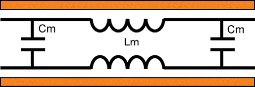
1: Mutual impedance between two traces on a PCB.
The mutual impedance is evenly distributed along both traces. Crosstalk is generated when a digital gate circuit generates a rising edge to the crosstalk line and propagates along the trace:
1. Both the mutual capacitance Cm and the mutual inductance Lm couple or "crosstalk" a voltage to the adjacent victim line.
2. The crosstalk voltage appears on the victim line as a narrow pulse with a width equal to the rise time of the pulse on the aggressor line.
3. On the victim line, the crosstalk pulse splits in two and then begins to propagate in two opposite directions. This separates the crosstalk into two components: forward crosstalk that propagates in the direction of the original aggressor pulse and reverse crosstalk that propagates in the opposite direction toward the signal source.
Crosstalk Types and Coupling Mechanisms
Based on the model discussed above, the coupling mechanism of crosstalk will be introduced below, and the two types of crosstalk, forward and reverse, will be discussed. Interference mechanism caused by mutual capacitance in
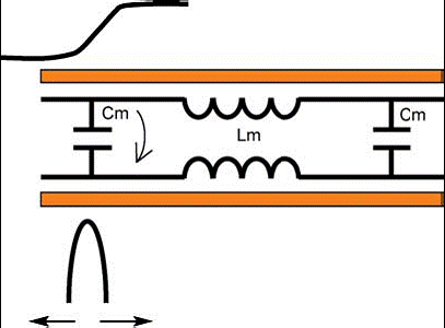
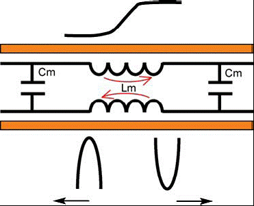
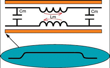
capacitive coupling mechanism circuit: >When the pulse on the interfering line reaches the capacitor, a narrow pulse will be coupled to the interfered line through the capacitor. >The amplitude of the coupled pulse is determined by the size of the mutual capacitance. >The coupled pulse is then split into two and begins to propagate in two opposite directions along the interfered line. Mutual inductance in inductive or transformer coupling mechanism circuits will cause the following interference: >The pulse propagating on the interfering line will charge the next location where the current spike appears. >This current spike will generate a magnetic field, which will then induce a current spike on the interfered line. >The transformer will generate two voltage spikes of opposite polarity on the interfered line: the negative spike propagates in the forward direction and the positive spike propagates in the reverse direction. Figure 2: Capacitive coupling crosstalk. Figure 3: Inductive coupling crosstalk. Figure 4: Reverse crosstalk. Figure 5: Forward crosstalk. Reverse Crosstalk The capacitive and inductive coupled crosstalk voltages resulting from the above model will add up at the crosstalk location of the victim line. The resulting reverse crosstalk has the following characteristics: > Reverse crosstalk is the sum of two pulses of the same polarity. > Since the crosstalk location propagates with the edge of the interfering pulse, the reverse interference appears as a low-level, wide pulse signal at the source of the victim line, and its width corresponds to the length of the trace. > The reflected crosstalk amplitude is independent of the rise time of the interfering line pulse, but depends on the mutual impedance value. Forward Crosstalk It is important to reiterate that the capacitive and inductive coupled crosstalk voltages will add up at the crosstalk location of the victim line. Forward crosstalk has the following characteristics: > Forward crosstalk is the sum of two pulses of opposite polarity. Because the polarity is opposite, the result depends on the relative values of capacitance and inductance. > Forward crosstalk appears as a narrow spike with a width equal to the rise time of the interfering pulse at the end of the victim line. > Forward crosstalk depends on the rise time of the interfering pulse. The faster the rise edge, the higher the amplitude and the narrower the width. >The forward crosstalk amplitude also depends on the line length: as the crosstalk position propagates along the edge of the interfering pulse, the forward crosstalk pulse on the interfered line will gain more energy. Characterization of Crosstalk This section will study the crosstalk generation mechanism and the several crosstalk types introduced above through several measurement examples on single-layer PCBs. Note: To familiarize yourself with crosstalk problems and their consequences on multi-layer PCBs and their ground planes, please read the references or other resources at the end of this article. Instrumentation and Setup

To effectively measure crosstalk in the lab, a wideband oscilloscope with a measurement bandwidth of 20 GHz should be used, and a high-quality pulse generator should be used to drive the circuit under test with a pulse output with a rise time equal to the oscilloscope rise time. High-quality cables, termination resistors, and adapters should also be used to connect the PCB under test. The
Tektronix 8000B Series instrument with the 80E04 electronic sampling module is the ideal instrument combination for successful crosstalk measurements. The 80E04 is a dual-channel sampling module that includes a TDR step voltage generator that can generate a narrow 250mv pulse with a rise time of 17ps and output it with a source impedance of 50 ohms. The tester only needs to connect the PCB under test.
Forward Crosstalk Measurement
If only forward crosstalk is measured, all traces need to be terminated to eliminate reflections. Forward crosstalk should be measured at the end of a well-terminated disturbed line. The instrument setup is shown in Figure 6.
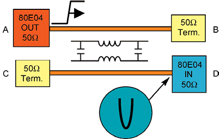
Figure 6: Measurement of forward crosstalk.
If the mutual inductance is greater than the mutual capacitance coupling crosstalk, then the crosstalk pulse should be negative at the rising edge of the interference pulse, and the width should be equal to the rise time of the interference pulse. The instrument shows a negative pulse (C4) with an amplitude of 48.45 mV. The interference pulse amplitude is 250 mV, while the crosstalk amplitude is nearly 50 mV, so the fast edge of the interference pulse generates 20% crosstalk on the interfered line. See Figure 7.
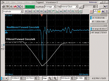
Figure 7: Measured forward crosstalk.
Because the input step voltage from the 80E04 has very fast edges during the measurement, the crosstalk is too large and does not represent the drive signal in the actual logic circuit. For example, if the drive signal comes from a 1.5 ns CMOS gate, the crosstalk pulse generated is wider and smaller in amplitude. To make the measurement reflect this situation, the Define Math function of the instrument can be used to add a low-pass filter after the signal capture. The M1 waveform (white) in Figure 7 shows the measurement result after filtering. Note that M1 is 10 times more sensitive in the vertical direction than the unfiltered waveform.
Although mathematical analysis has proven that the effect of low-pass filtering after signal capture is the same as physically filtering the interference pulse connected to the line, the following measurements are more convincing:
>Measure the crosstalk caused by two interference pulses with the same amplitude, one fast and one slow.
>Then low-pass filter the crosstalk caused by the fast interference pulse to the crosstalk caused by the slow interference pulse, and finally check the result.
Figure 8 shows the measurement results displayed on the instrument:
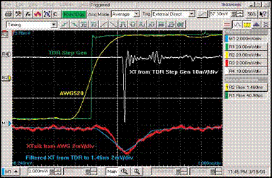
Figure 8: Post-filtering of forward crosstalk.
>The yellow waveform (R2) is the slow interference pulse, and the red waveform (R3) is the crosstalk caused by it.
>The green waveform is the fast TDR pulse (R1), and the white waveform (R4) is the crosstalk caused by it.
>The blue waveform is the waveform obtained by filtering the white waveform and slowing down the pulse rising edge. It represents the result of post-filtering the crosstalk. The red and blue crosstalk waveforms shown in the figure are displayed on the same voltage scale.
Reverse crosstalk measurement
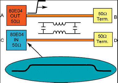
Figure 9: Reverse crosstalk measurement.
When measuring reverse crosstalk alone, both the interfering line and the interfered line need to be terminated with a 50 ohm resistor to eliminate reflection. The measurement should be performed at the left end of the interfered line, as shown in Figure 9. The amplitude of the reflected pulse is very low, and the width is twice the line length, because the crosstalk at the end of the line must be transmitted back to the source end of the line. Figure ?? shows the measurement of reverse crosstalk. The crosstalk generated by the fast-edge interference pulse in the figure is about ?? mV, which is equivalent to 4% of the amplitude of the interference pulse. The amplitude of the reverse crosstalk has nothing to do with the rise time of the interference pulse. In Figure 10, the following two waveforms are the waveforms obtained by post-filtering the crosstalk generated by the slow-edge pulse and the crosstalk generated by the fast-edge pulse. Their amplitudes are both 6.5 mV. The difference between the line length and the rise time of the interference pulse makes the reverse crosstalk amplitude generated by the slow-edge pulse smaller.
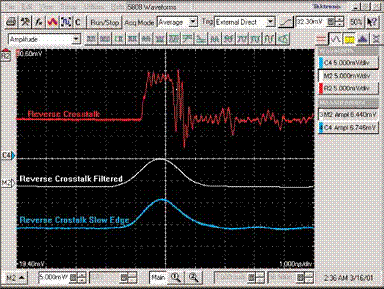
Figure 10: Measured reverse crosstalk.
Because the rise time of the interference pulse is greater than the line length at this time, the pulse edge has not reached the peak of the amplitude when it is transmitted back to the source end of the line along the line direction. Figure 11 shows the crosstalk measurement results when using a 200 ps rise time generator (DG2040) and the output of the 17 ps generator of the 80E04 sampling module as interference pulses. The three crosstalk waveforms shown in the figure all use a voltage scale of 5 mV/div.
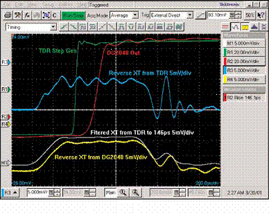
Figure 11: Reverse crosstalk is independent of signal rise time.
The white waveform is the crosstalk generated by the interference pulse with a rise time of 17 ps, which is filtered (post filtering) to a rise time of 200 ps by the waveform operation function. These measurements confirm that unless the rise time of the interference pulse exceeds the length of the trace, the rise time does not affect the reverse crosstalk. If the rise time of the interference pulse exceeds the length of the trace, the reverse crosstalk amplitude is small because in this case the pulse edge cannot reach the peak amplitude before traveling the entire trace. The
impact of circuit design on crosstalk
Although crosstalk can be reduced and its effects can be weakened or eliminated through careful PCB design, some crosstalk may still remain on the board. Therefore, when designing a circuit, you should also use appropriate end loads, because end loads affect the size of the crosstalk and the degree to which the crosstalk weakens over time. Below is a measurement example that reveals how end loads at the end of the trace and at the output of the logic gate circuit attenuate the crosstalk and reduce the causes of crosstalk.
Reference address:Time Domain Crosstalk Measurement for PCB Quality Verification
As digital systems in the fields of communications, video, networking, and computer technology run faster and faster, the quality requirements for printed circuit boards (PCBs) in such systems are also getting higher and higher. Early PCB designs could no longer guarantee system performance and operating requirements in the face of increasing signal frequencies and decreasing pulse rise times. In today's PCB design, we need to use transmission line theory to model the PCB and its components (edge connectors, microstrip lines, and component sockets). Only by fully understanding the forms, mechanisms, and consequences of crosstalk on PCBs and using appropriate techniques to minimize it can we help improve the reliability of systems that include PCBs. This article focuses on PCB design, but I believe that the content discussed in this article is also helpful for other applications such as cable and connector characterization.
Possible Consequences of Crosstalk
PCB designers are concerned about crosstalk because it can cause the following performance issues:
> Increased noise levels,
> Unwanted spikes and glitches,
> Data edge jitter,
> Unexpected signal reflections.
Which of these issues will affect the PCB design depends on many factors, such as the characteristics of the logic circuits used on the board, the design of the board, the mode of crosstalk (reverse or forward), and the termination conditions on both the aggressor and the victim lines. The information provided below can help readers deepen their understanding and study of crosstalk and reduce its impact on the design.
Methods for Studying Crosstalk
To minimize crosstalk in PCB design, we must find a balance between capacitive reactance and inductive reactance and strive to achieve the rated impedance value because the manufacturability of the PCB requires that the transmission line impedance be well controlled. After the board design is completed, the components, connectors, and termination methods on the board determine how much impact each type of crosstalk will have on the circuit performance. Using time domain measurements, calculating the inflection point frequency and understanding the PCB crosstalk (Crosstalk-on-PCB) model can help designers set the boundaries for crosstalk analysis.
Time Domain Measurement Methods
To measure and analyze crosstalk, frequency domain techniques can be used to observe the relationship between the harmonic components of the clock in the spectrum and the maximum EMI at these harmonic frequencies. However, time domain measurements of digital signal edges (the time it takes for the signal level to rise from 10% to 90%) are also a means of measuring and analyzing crosstalk, and time domain measurements have the following advantages: The speed of change of the digital signal edge, or rise time, directly reflects how high each frequency component in the signal is. Therefore, the signal speed defined by the signal edge (i.e., rise time) can also help reveal the mechanism of crosstalk. Rise time can be directly used to calculate the inflection point frequency. This article will use the rise time measurement method to explain and measure crosstalk.
Inflection Point Frequency
To ensure that a digital system can work reliably, designers must study and verify the performance of the circuit design below the inflection point frequency. Frequency domain analysis of digital signals shows that signals above the inflection point frequency are attenuated and have no substantial impact on crosstalk, while signals below the inflection point frequency contain enough energy to affect circuit operation. The knee frequency is calculated by the following equation:
fknee = 0.5/ trise
PCB Crosstalk Model
The model presented in this section provides a platform for studying different forms of crosstalk and illustrates how the mutual impedance between two microstrip lines causes crosstalk on a PCB. Figure 1 is a conceptual mutual impedance model. Figure

1: Mutual impedance between two traces on a PCB.
The mutual impedance is evenly distributed along both traces. Crosstalk is generated when a digital gate circuit generates a rising edge to the crosstalk line and propagates along the trace:
1. Both the mutual capacitance Cm and the mutual inductance Lm couple or "crosstalk" a voltage to the adjacent victim line.
2. The crosstalk voltage appears on the victim line as a narrow pulse with a width equal to the rise time of the pulse on the aggressor line.
3. On the victim line, the crosstalk pulse splits in two and then begins to propagate in two opposite directions. This separates the crosstalk into two components: forward crosstalk that propagates in the direction of the original aggressor pulse and reverse crosstalk that propagates in the opposite direction toward the signal source.
Crosstalk Types and Coupling Mechanisms
Based on the model discussed above, the coupling mechanism of crosstalk will be introduced below, and the two types of crosstalk, forward and reverse, will be discussed. Interference mechanism caused by mutual capacitance in
capacitive coupling mechanism circuit: >When the pulse on the interfering line reaches the capacitor, a narrow pulse will be coupled to the interfered line through the capacitor. >The amplitude of the coupled pulse is determined by the size of the mutual capacitance. >The coupled pulse is then split into two and begins to propagate in two opposite directions along the interfered line. Mutual inductance in inductive or transformer coupling mechanism circuits will cause the following interference: >The pulse propagating on the interfering line will charge the next location where the current spike appears. >This current spike will generate a magnetic field, which will then induce a current spike on the interfered line. >The transformer will generate two voltage spikes of opposite polarity on the interfered line: the negative spike propagates in the forward direction and the positive spike propagates in the reverse direction. Figure 2: Capacitive coupling crosstalk. Figure 3: Inductive coupling crosstalk. Figure 4: Reverse crosstalk. Figure 5: Forward crosstalk. Reverse Crosstalk The capacitive and inductive coupled crosstalk voltages resulting from the above model will add up at the crosstalk location of the victim line. The resulting reverse crosstalk has the following characteristics: > Reverse crosstalk is the sum of two pulses of the same polarity. > Since the crosstalk location propagates with the edge of the interfering pulse, the reverse interference appears as a low-level, wide pulse signal at the source of the victim line, and its width corresponds to the length of the trace. > The reflected crosstalk amplitude is independent of the rise time of the interfering line pulse, but depends on the mutual impedance value. Forward Crosstalk It is important to reiterate that the capacitive and inductive coupled crosstalk voltages will add up at the crosstalk location of the victim line. Forward crosstalk has the following characteristics: > Forward crosstalk is the sum of two pulses of opposite polarity. Because the polarity is opposite, the result depends on the relative values of capacitance and inductance. > Forward crosstalk appears as a narrow spike with a width equal to the rise time of the interfering pulse at the end of the victim line. > Forward crosstalk depends on the rise time of the interfering pulse. The faster the rise edge, the higher the amplitude and the narrower the width. >The forward crosstalk amplitude also depends on the line length: as the crosstalk position propagates along the edge of the interfering pulse, the forward crosstalk pulse on the interfered line will gain more energy. Characterization of Crosstalk This section will study the crosstalk generation mechanism and the several crosstalk types introduced above through several measurement examples on single-layer PCBs. Note: To familiarize yourself with crosstalk problems and their consequences on multi-layer PCBs and their ground planes, please read the references or other resources at the end of this article. Instrumentation and Setup


To effectively measure crosstalk in the lab, a wideband oscilloscope with a measurement bandwidth of 20 GHz should be used, and a high-quality pulse generator should be used to drive the circuit under test with a pulse output with a rise time equal to the oscilloscope rise time. High-quality cables, termination resistors, and adapters should also be used to connect the PCB under test. The
Tektronix 8000B Series instrument with the 80E04 electronic sampling module is the ideal instrument combination for successful crosstalk measurements. The 80E04 is a dual-channel sampling module that includes a TDR step voltage generator that can generate a narrow 250mv pulse with a rise time of 17ps and output it with a source impedance of 50 ohms. The tester only needs to connect the PCB under test.
Forward Crosstalk Measurement
If only forward crosstalk is measured, all traces need to be terminated to eliminate reflections. Forward crosstalk should be measured at the end of a well-terminated disturbed line. The instrument setup is shown in Figure 6.

Figure 6: Measurement of forward crosstalk.
If the mutual inductance is greater than the mutual capacitance coupling crosstalk, then the crosstalk pulse should be negative at the rising edge of the interference pulse, and the width should be equal to the rise time of the interference pulse. The instrument shows a negative pulse (C4) with an amplitude of 48.45 mV. The interference pulse amplitude is 250 mV, while the crosstalk amplitude is nearly 50 mV, so the fast edge of the interference pulse generates 20% crosstalk on the interfered line. See Figure 7.

Figure 7: Measured forward crosstalk.
Because the input step voltage from the 80E04 has very fast edges during the measurement, the crosstalk is too large and does not represent the drive signal in the actual logic circuit. For example, if the drive signal comes from a 1.5 ns CMOS gate, the crosstalk pulse generated is wider and smaller in amplitude. To make the measurement reflect this situation, the Define Math function of the instrument can be used to add a low-pass filter after the signal capture. The M1 waveform (white) in Figure 7 shows the measurement result after filtering. Note that M1 is 10 times more sensitive in the vertical direction than the unfiltered waveform.
Although mathematical analysis has proven that the effect of low-pass filtering after signal capture is the same as physically filtering the interference pulse connected to the line, the following measurements are more convincing:
>Measure the crosstalk caused by two interference pulses with the same amplitude, one fast and one slow.
>Then low-pass filter the crosstalk caused by the fast interference pulse to the crosstalk caused by the slow interference pulse, and finally check the result.
Figure 8 shows the measurement results displayed on the instrument:

Figure 8: Post-filtering of forward crosstalk.
>The yellow waveform (R2) is the slow interference pulse, and the red waveform (R3) is the crosstalk caused by it.
>The green waveform is the fast TDR pulse (R1), and the white waveform (R4) is the crosstalk caused by it.
>The blue waveform is the waveform obtained by filtering the white waveform and slowing down the pulse rising edge. It represents the result of post-filtering the crosstalk. The red and blue crosstalk waveforms shown in the figure are displayed on the same voltage scale.
Reverse crosstalk measurement

Figure 9: Reverse crosstalk measurement.
When measuring reverse crosstalk alone, both the interfering line and the interfered line need to be terminated with a 50 ohm resistor to eliminate reflection. The measurement should be performed at the left end of the interfered line, as shown in Figure 9. The amplitude of the reflected pulse is very low, and the width is twice the line length, because the crosstalk at the end of the line must be transmitted back to the source end of the line. Figure ?? shows the measurement of reverse crosstalk. The crosstalk generated by the fast-edge interference pulse in the figure is about ?? mV, which is equivalent to 4% of the amplitude of the interference pulse. The amplitude of the reverse crosstalk has nothing to do with the rise time of the interference pulse. In Figure 10, the following two waveforms are the waveforms obtained by post-filtering the crosstalk generated by the slow-edge pulse and the crosstalk generated by the fast-edge pulse. Their amplitudes are both 6.5 mV. The difference between the line length and the rise time of the interference pulse makes the reverse crosstalk amplitude generated by the slow-edge pulse smaller.

Figure 10: Measured reverse crosstalk.
Because the rise time of the interference pulse is greater than the line length at this time, the pulse edge has not reached the peak of the amplitude when it is transmitted back to the source end of the line along the line direction. Figure 11 shows the crosstalk measurement results when using a 200 ps rise time generator (DG2040) and the output of the 17 ps generator of the 80E04 sampling module as interference pulses. The three crosstalk waveforms shown in the figure all use a voltage scale of 5 mV/div.

Figure 11: Reverse crosstalk is independent of signal rise time.
The white waveform is the crosstalk generated by the interference pulse with a rise time of 17 ps, which is filtered (post filtering) to a rise time of 200 ps by the waveform operation function. These measurements confirm that unless the rise time of the interference pulse exceeds the length of the trace, the rise time does not affect the reverse crosstalk. If the rise time of the interference pulse exceeds the length of the trace, the reverse crosstalk amplitude is small because in this case the pulse edge cannot reach the peak amplitude before traveling the entire trace. The
impact of circuit design on crosstalk
Although crosstalk can be reduced and its effects can be weakened or eliminated through careful PCB design, some crosstalk may still remain on the board. Therefore, when designing a circuit, you should also use appropriate end loads, because end loads affect the size of the crosstalk and the degree to which the crosstalk weakens over time. Below is a measurement example that reveals how end loads at the end of the trace and at the output of the logic gate circuit attenuate the crosstalk and reduce the causes of crosstalk.
Previous article:Three Methods for Jitter Measurement
Next article:Mix and Match Test/Measurement Buses and Hybrid Systems
- Popular Resources
- Popular amplifiers
Recommended Content
Latest Test Measurement Articles
- Keysight Technologies Helps Samsung Electronics Successfully Validate FiRa® 2.0 Safe Distance Measurement Test Case
- From probes to power supplies, Tektronix is leading the way in comprehensive innovation in power electronics testing
- Seizing the Opportunities in the Chinese Application Market: NI's Challenges and Answers
- Tektronix Launches Breakthrough Power Measurement Tools to Accelerate Innovation as Global Electrification Accelerates
- Not all oscilloscopes are created equal: Why ADCs and low noise floor matter
- Enable TekHSI high-speed interface function to accelerate the remote transmission of waveform data
- How to measure the quality of soft start thyristor
- How to use a multimeter to judge whether a soft starter is good or bad
- What are the advantages and disadvantages of non-contact temperature sensors?
MoreSelected Circuit Diagrams
MorePopular Articles
- Innolux's intelligent steer-by-wire solution makes cars smarter and safer
- 8051 MCU - Parity Check
- How to efficiently balance the sensitivity of tactile sensing interfaces
- What should I do if the servo motor shakes? What causes the servo motor to shake quickly?
- 【Brushless Motor】Analysis of three-phase BLDC motor and sharing of two popular development boards
- Midea Industrial Technology's subsidiaries Clou Electronics and Hekang New Energy jointly appeared at the Munich Battery Energy Storage Exhibition and Solar Energy Exhibition
- Guoxin Sichen | Application of ferroelectric memory PB85RS2MC in power battery management, with a capacity of 2M
- Analysis of common faults of frequency converter
- In a head-on competition with Qualcomm, what kind of cockpit products has Intel come up with?
- Dalian Rongke's all-vanadium liquid flow battery energy storage equipment industrialization project has entered the sprint stage before production
MoreDaily News
- Allegro MicroSystems Introduces Advanced Magnetic and Inductive Position Sensing Solutions at Electronica 2024
- Car key in the left hand, liveness detection radar in the right hand, UWB is imperative for cars!
- After a decade of rapid development, domestic CIS has entered the market
- Aegis Dagger Battery + Thor EM-i Super Hybrid, Geely New Energy has thrown out two "king bombs"
- A brief discussion on functional safety - fault, error, and failure
- In the smart car 2.0 cycle, these core industry chains are facing major opportunities!
- The United States and Japan are developing new batteries. CATL faces challenges? How should China's new energy battery industry respond?
- Murata launches high-precision 6-axis inertial sensor for automobiles
- Ford patents pre-charge alarm to help save costs and respond to emergencies
- New real-time microcontroller system from Texas Instruments enables smarter processing in automotive and industrial applications
Guess you like
- MCU Programming_Interrupt
- Using TI power timing controller in 5G MIMO application
- MCU development full-time/part-time and sales assistant
- G100 acoustic imager is used in many product development and fault diagnosis fields
- The moon rises over the sea, and the world is sharing this moment
- Treatment of cross-partition area and slot in EMC design of power board
- Resistor Accuracy and Temperature Drift
- Multisum circuit simulation has problems
- The use of archiver in DSP
- Dealing with the noise of switching power supply from three aspects

 Multi-port and shared memory architecture for high-performance ADAS SoCs
 CVPR 2023 Paper Summary: Vision Applications and Systems


 京公网安备 11010802033920号