Jitter amplifier circuit design architecture [7] [8]
"Figure 9 Jitter amplifier circuit architecture and timing diagram"
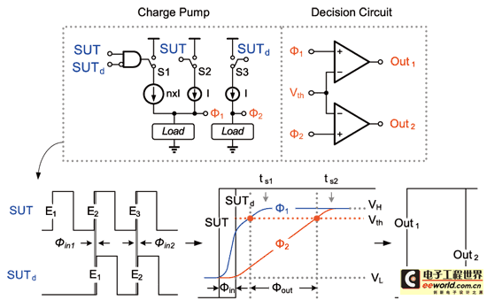
The cycle-to-cycle jitter is the phase error between the edge En+1 of the next cycle and the edge En of the previous cycle. Therefore, if the jitter amplification is to be achieved, the edge time difference between En and En+1 must be widened. In this article, the principle of current charging and discharging of the load will be used to achieve the function of jitter amplification. We use Figure 9 to illustrate its operating principle.
The jitter amplifier circuit is basically composed of two sets of charge pumps (CP) with different current amounts and decision circuits (DC), which are controlled by the signal under test SUT, the signal SUTd after one cycle delay, and the combination of the two. The most basic idea is to use different charging slopes (i.e. charging speed) with different starting points (i.e. transition edges) of the signal to synthesize a clock edge with a larger jitter. In order to explain the amplification principle clearly, we divide SUT (S) and SUTd (Sd) into four intervals according to the phase relationship, and then discuss the operation conditions in different intervals. As shown in Table 1.
(Table 1) Charge pump operation state table
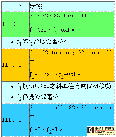
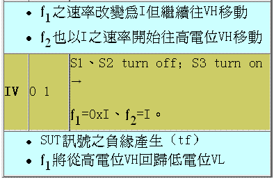
with Figure 9 and Table 1, it can be seen that in the initial state, because SUT and SUTd are at low potential, the switches are turned off, so there is no current to charge the load, so the output result (f1, f2) will be low potential (VL). But if there is jitter between the two phases, SUT will be high potential and SUTd will be low potential. At this time, f1 will charge the load with (n+1) times the current to pull up, and f2 will maintain the low potential of the previous state because S3 turns off. Then after a period of Δτ, SUTd also pulls high, prompting S3 to turn on and S1 to turn off. At this time, f1 and f2 will move to a high potential together at a speed of I. But if you look closely at Region II and Region II, III process, because f1 starts at a faster speed during the period of Δτ, if Region III is under the same charging slope condition (the current is all I), it will reach the steady-state level first; and then after n*Δτ time, f2 will also reach this level. At this time, it can be seen from Figure 9 that f1, f2 and the set critical voltage (Vth) have two intersections. If two sets of decision circuits are used to determine the transition point, two sets of output signals with different phase differences (Out1, Out2) can be generated. Therefore, using the above conditions, we can simply use Formula 1 to express the relationship between output and input:
《Formula 1》
Where fOUT is the phase difference between Out1 and Out2 (the cycle-to-cycle jitter after amplification), fIN is the phase difference between SUT and SUTd (the cycle-to-cycle jitter before amplification), and A represents the amplification factor.
Using the above concepts, this creation can amplify the cycle-to-cycle jitter of the clock signal to make up for the shortcomings of the time-to-digital conversion circuit. However, relying solely on the behavior mode of current charging capability to achieve the purpose of amplification will face circuit operation bottlenecks and lead to test errors, such as nonlinearity of the amplification factor or changes in operating frequency. Next, we will propose solutions to these effects.
Analysis of jitter amplification circuit and pulse remover design
(Table 2) Symbols represent that
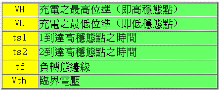
in the basic design of the jitter amplifier circuit, because the current is used to charge and discharge the load to achieve jitter amplification, the charge and discharge level and time are defined first. As shown in Table 2.
In Figure 10 (a), when the jitter amplifier circuit is usually operated at a low rate, because the jitter amount is smaller than the proportion of the half cycle time, the time for the charge pump output (f1, f2) to reach the high steady-state point (ts1, ts2) is usually less than the negative edge transition point time tf. [page]
《Figure 10 Jitter amplifier circuit timing diagram: (a) Case 1: tf>ts2; (b) Case 2: tf≈ts2; (c) Case 3: tf
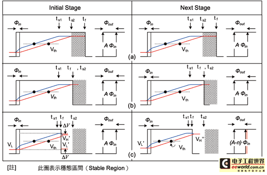
Therefore, in this frequency band, there is enough stable region, and the output phase difference fOUT generated after the decision circuit can almost maintain a constant value compared to the input phase difference fIN, which means that the amplification factor A is constant. However, if the measured clock frequency increases, as shown in Figure 10 (b), the occurrence point of tf is advanced as the signal period is shortened. When tf is very close to but greater than ts2, the jitter amplifier circuit can still barely maintain the amplification factor, so this time is called the operating critical value. However, if unfortunately tf varies greatly in the application used or the operating frequency continues to increase, causing ts2 to occur later than tf, the amplification factor will begin to change nonlinearly.
From Figure 10 (c), it can be observed that under normal operating mode, f1 and f2 will eventually return to the steady-state level VH and VL. However, if the transition edge tf appears before it stabilizes, the voltages of f1 and f2 will be forced to maintain at the new level, that is, VH' (=VH-ΔV) and VL' (=VL +ΔV). Although this phenomenon has no effect on the gain of the first cycle (initial stage), it can be seen from the figure that in the next cycle (next stage), because the starting voltage level of f1 and f2 has changed, the intersection point with the critical voltage Vth after charging will inevitably change accordingly. In other words, the voltage domain variation will be converted into the phase error of the time domain, which will cause the gain to change. Therefore, when the cycle-to-cycle jitter amplifier circuit needs to operate in a wide range application, it is necessary to use some mechanism to control the steady-state time point ts to occur earlier than the negative edge transition point tf, so as not to cause distortion of the gain. In view of this, this article will propose a single-capture measurement method using the concept of pulse swallowing to improve it.
Single-capture measurement method of pulse swallowing
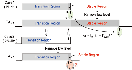
[Figure 11 Pulse swallowing concept diagram]
As can be seen from the above discussion, if tsf is to be achieved, it is nothing more than pulling the steady-state time point forward or delaying the time when the negative edge transition point occurs. From the perspective of circuit implementation, ts is the intersection of the voltage generated by the current after charging the load and the high potential VH. Therefore, the larger the current, the stronger the ability to return to the steady-state point, and the earlier it will appear. However, the jitter amplification is generated by the difference between currents of different rates, and the amplification factor will inevitably be affected. Therefore, in order to balance the trade-off between the amplification factor and the current, this article will use the method of delaying tf to maintain the jitter amplification factor under different operating frequencies.
As shown in Figure 11, case 1 is a schematic diagram of low-frequency operation. In order to keep the amplification factor of the jitter amplifier circuit constant, the ts of the signal to be tested must be less than tf, and the worst case will occur at the time point when ts is equal to tf. At this time, the steady-state interval will almost be close to zero, which means that the amplification factor will be very unstable.
In order to improve this problem, according to the previous statement, the tf time point must be delayed. Simply put, it is to slow down the test speed and use the pulse swallowing circuit to remove 0.5 cycles in exchange for the width of the steady-state interval. As shown in the figure, if the signal of case 1 is processed to become TAIn1, the time when its negative edge transition occurs is delayed by Δτ (=tfn-tf=Tcycle/2), which means that the steady-state interval is enlarged by 2 times. Therefore, if the frequency of the signal to be measured is increased, it has enough steady-state time, so the amplification factor will not be affected by clock variation and frequency change.
However, in Case 2 of Figure 11, the operating speed of the clock signal to be tested continues to increase (about twice that of Case 1). It can be clearly observed that if the pulse swallowing mechanism is not used, ts has far exceeded tf. At this time, the amplification factor of the jitter amplifier circuit has become a nonlinear operation; but if the pulse swallowing mechanism is added, because the speed of the signal to be tested is too fast, under the same charging and discharging rate conditions, ts is also very close to tfn, and the problem of amplification factor variation still exists. Therefore, it can be seen that in order to truly achieve wide range operation, no matter at any frequency, it is necessary to have the same steady-state range to truly obtain a constant amplification factor. In view of this, we will slightly modify the pulse swallowing mechanism and will no longer maintain a fixed removal of 0.5 cycles, but will change with each doubling of the frequency of the object to be tested. The remove number can be expressed by Formula 2:
Formula 2
Where N is the frequency change rate. In the example presented in this article, 100MHz is used as the benchmark because the operation range is from tens of MHz to 1.6GHz. Every time the frequency doubles, the remove number must be changed to maintain the amplification factor. This is shown in Figure 12.
"Figure 12 is a conceptual diagram of pulse swallowing between various operating frequency bands."
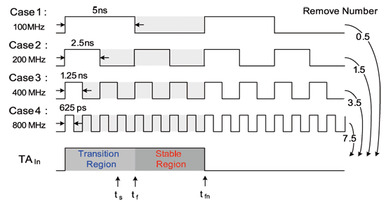
From the perspective of circuits, it is not difficult to implement the pulse swallowing circuit in Figure 12. It can be achieved by passing the measured signal through the corresponding frequency divider according to the frequency band. However, in fact, if the measured signal is directly passed through the frequency divider to achieve pulse swallowing, according to reference [9], the jitter of the signal will also be amplified at the same time, by about √n times. In addition, the circuit divided by 16 requires at least 4 sets of DFFs to implement, which means that the measured signal must pass through many transistors before reaching the jitter amplifier circuit, and then be interfered by power noise or thermal noise, resulting in increased jitter, which will seriously affect the measurement accuracy. [page]
Using edge detection to achieve pulse swallowing effect
[Figure 13 (a) Jitter amplifier circuit proposed; (b) Schematic diagram of edge detection circuit operation]
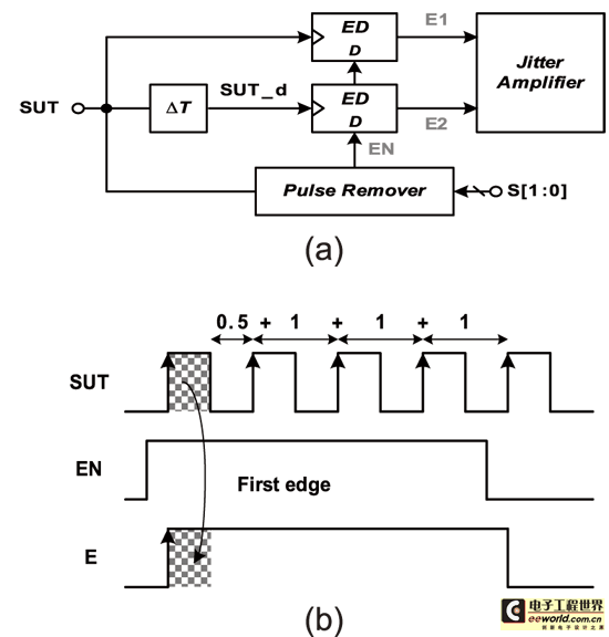
Therefore, this article will use edge detection technology to achieve the effect of pulse swallowing, as shown in Figure 13 (a). It mainly includes two blocks: edge detector and pulse swallowing circuit. First, when the signal to be tested is activated, in order to maintain the amplification factor, the pulse remove action must be performed first. Taking Figure 13 (b) as an example, SUT is the signal to be tested, EN is generated by the pulse swallowing circuit, and E is the processed signal to be tested. The pulse swallowing circuit is implemented by MUX, which can select the EN signal as the result of /2, /4, /8, /16 of SUT by controlling the s pin.
In addition, EN is connected to the data input terminal of the edge detector, and SUT is connected to the clock input terminal. When EN is high, SUT will sample Hi after the positive edge is generated, so the signal E will immediately pull Hi. If we choose to remove /8 at this time, as shown in Case 3 of Figure 12, the EN signal will maintain a time of 4*TSUT and then turn to a low potential. Therefore, when the next positive edge of the SUT is generated, it will sample to Low, causing the signal E to pull down.
It can be seen from the figure that the signal SUT successfully removes 3.5 (=4-0.5) cycles after conversion, and the SUT signal only passes through one ED. In this way, the stable region can be lengthened, the amplification factor can be maintained, and the original jitter amount will not be changed due to making the path of the signal to be tested too long. Therefore, using the jitter amplification technology proposed above and the single-capture measurement method of the pulse swallowing concept, the jitter of the clock pulse to be tested can be linearly amplified in any frequency band, so as to facilitate the jitter analysis of the subsequent time-to-digital conversion circuit and solve the problem of insufficient accuracy caused by process limitations.
Time-to-Digital Converter (TDC) Time-to-Digital Converter (TDC)
as shown in Figure 14
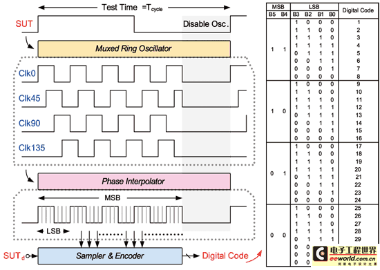
In this paper, we propose a new time-to-digital converter circuit. This is because traditional time-to-digital converter circuits basically use multi-stage buffers or delay units to generate multi-phase signals, and then obtain digital codes by sampling. However, with the current 0.13-um process, the minimum buffer delay that can be generated is about 25-ps; that is, from the perspective of the entire system, the highest resolution that can be tested is also equal to 25-ps. This specification can no longer meet the test requirements in today's high-speed applications.
In view of this, we will use a multiplexed oscillator with a phase interpolation method to realize a higher resolution time-to-digital converter circuit. As shown in Figure 14. It mainly includes a set of multiplexed oscillators (Muxed oscillator), a phase interpolator circuit (Phase Interpolator; PI) and a sampling encoding circuit, in which the multiplexed oscillator is used to generate a multi-phase reference signal. Compared with the traditional open loop delay chain, the close loop has a feedback mechanism, so it has a more accurate unit delay time and is less susceptible to process drift. In addition, because the phase is generated by the oscillation principle, the unit delay time can be calculated by testing the oscillation frequency. If the interpolation circuit technology is then used, the test resolution can be greatly improved. "
Figure 15 Circuit structure diagram of multiplexed oscillator"
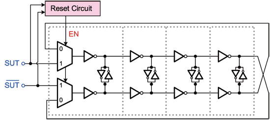
The multiplexed oscillator is the most important circuit in the time-to-digital conversion circuit, because it must oscillate the multi-phase high-speed signal used for sampling according to the rising edge of the signal to be tested. As shown in Figure 15, it consists of two multiplexers, four-stage delay units and a reset circuit. It is called a multiplexed oscillator because this circuit has two operating modes, namely oscillating mode and latching mode, and the mode switching is determined by the reset circuit.
The relevant operating principle is as follows. When the positive edge of the signal to be tested is generated, the reset circuit will output EN as a low circuit, and the multiplexer selects 0 at this time. As shown in Figure 15, the loop can be regarded as a differential oscillator, which continuously and stably provides multi-phase high-speed reference signals. However, the jitter amount in each system usually does not exceed half a cycle, that is, (1/2) xUI, so in fact the jitter test in each cycle will be completed within half a cycle, so it is only necessary to generate the sampled signal in half a cycle of the circuit under test. In other words, the multiplexed oscillator only needs to work for half a cycle before it can be turned off.
Therefore, when the negative edge of the signal under test occurs, the reset circuit will force EN to a high potential, and the multiplexer will output from the path of 1, that is, switch to the latch mode. It can be seen from the figure that the overall oscillation loop has been cut off at this time, and the input is the signal under test. The output of each delay unit is either the delay of the signal under test or the reverse delay of the signal under test. The oscillation mode will not be restored until the positive edge is generated again to facilitate the jitter test.
The design of traditional time-to-digital conversion circuits is usually limited by the minimum gate delay that the process can produce. To overcome this problem, we use a common phase interpolation circuit to generate a delay time that is less than that provided by a delay unit. The intuitive idea of the phase interpolation circuit is to generate a new signal between two adjacent phase signals, and its phase will be between the two adjacent phase signals, thereby achieving a signal with higher phase resolution [10].
Summary
The above introduces the idea and architecture of built-in jitter testing. The main purpose is to solve the problem that traditional testing methods cannot test low jitter by amplifying the input jitter, and to improve the overall system resolution by combining it with a multiplexed oscillator time-to-digital conversion circuit. In addition, a pulse swallowing circuit is proposed based on the circuit operation characteristics, so that this test system can perform self-tests in each frequency band, and the test quality will not be affected by the operation speed. In the next chapter, we will use HSpice to verify the proposed method and architecture.
Reference address:Built-in jitter measurement technology (Part 2)
"Figure 9 Jitter amplifier circuit architecture and timing diagram"

The cycle-to-cycle jitter is the phase error between the edge En+1 of the next cycle and the edge En of the previous cycle. Therefore, if the jitter amplification is to be achieved, the edge time difference between En and En+1 must be widened. In this article, the principle of current charging and discharging of the load will be used to achieve the function of jitter amplification. We use Figure 9 to illustrate its operating principle.
The jitter amplifier circuit is basically composed of two sets of charge pumps (CP) with different current amounts and decision circuits (DC), which are controlled by the signal under test SUT, the signal SUTd after one cycle delay, and the combination of the two. The most basic idea is to use different charging slopes (i.e. charging speed) with different starting points (i.e. transition edges) of the signal to synthesize a clock edge with a larger jitter. In order to explain the amplification principle clearly, we divide SUT (S) and SUTd (Sd) into four intervals according to the phase relationship, and then discuss the operation conditions in different intervals. As shown in Table 1.
(Table 1) Charge pump operation state table


with Figure 9 and Table 1, it can be seen that in the initial state, because SUT and SUTd are at low potential, the switches are turned off, so there is no current to charge the load, so the output result (f1, f2) will be low potential (VL). But if there is jitter between the two phases, SUT will be high potential and SUTd will be low potential. At this time, f1 will charge the load with (n+1) times the current to pull up, and f2 will maintain the low potential of the previous state because S3 turns off. Then after a period of Δτ, SUTd also pulls high, prompting S3 to turn on and S1 to turn off. At this time, f1 and f2 will move to a high potential together at a speed of I. But if you look closely at Region II and Region II, III process, because f1 starts at a faster speed during the period of Δτ, if Region III is under the same charging slope condition (the current is all I), it will reach the steady-state level first; and then after n*Δτ time, f2 will also reach this level. At this time, it can be seen from Figure 9 that f1, f2 and the set critical voltage (Vth) have two intersections. If two sets of decision circuits are used to determine the transition point, two sets of output signals with different phase differences (Out1, Out2) can be generated. Therefore, using the above conditions, we can simply use Formula 1 to express the relationship between output and input:
《Formula 1》

Where fOUT is the phase difference between Out1 and Out2 (the cycle-to-cycle jitter after amplification), fIN is the phase difference between SUT and SUTd (the cycle-to-cycle jitter before amplification), and A represents the amplification factor.
Using the above concepts, this creation can amplify the cycle-to-cycle jitter of the clock signal to make up for the shortcomings of the time-to-digital conversion circuit. However, relying solely on the behavior mode of current charging capability to achieve the purpose of amplification will face circuit operation bottlenecks and lead to test errors, such as nonlinearity of the amplification factor or changes in operating frequency. Next, we will propose solutions to these effects.
Analysis of jitter amplification circuit and pulse remover design
(Table 2) Symbols represent that

in the basic design of the jitter amplifier circuit, because the current is used to charge and discharge the load to achieve jitter amplification, the charge and discharge level and time are defined first. As shown in Table 2.
In Figure 10 (a), when the jitter amplifier circuit is usually operated at a low rate, because the jitter amount is smaller than the proportion of the half cycle time, the time for the charge pump output (f1, f2) to reach the high steady-state point (ts1, ts2) is usually less than the negative edge transition point time tf. [page]
《Figure 10 Jitter amplifier circuit timing diagram: (a) Case 1: tf>ts2; (b) Case 2: tf≈ts2; (c) Case 3: tf

Therefore, in this frequency band, there is enough stable region, and the output phase difference fOUT generated after the decision circuit can almost maintain a constant value compared to the input phase difference fIN, which means that the amplification factor A is constant. However, if the measured clock frequency increases, as shown in Figure 10 (b), the occurrence point of tf is advanced as the signal period is shortened. When tf is very close to but greater than ts2, the jitter amplifier circuit can still barely maintain the amplification factor, so this time is called the operating critical value. However, if unfortunately tf varies greatly in the application used or the operating frequency continues to increase, causing ts2 to occur later than tf, the amplification factor will begin to change nonlinearly.
From Figure 10 (c), it can be observed that under normal operating mode, f1 and f2 will eventually return to the steady-state level VH and VL. However, if the transition edge tf appears before it stabilizes, the voltages of f1 and f2 will be forced to maintain at the new level, that is, VH' (=VH-ΔV) and VL' (=VL +ΔV). Although this phenomenon has no effect on the gain of the first cycle (initial stage), it can be seen from the figure that in the next cycle (next stage), because the starting voltage level of f1 and f2 has changed, the intersection point with the critical voltage Vth after charging will inevitably change accordingly. In other words, the voltage domain variation will be converted into the phase error of the time domain, which will cause the gain to change. Therefore, when the cycle-to-cycle jitter amplifier circuit needs to operate in a wide range application, it is necessary to use some mechanism to control the steady-state time point ts to occur earlier than the negative edge transition point tf, so as not to cause distortion of the gain. In view of this, this article will propose a single-capture measurement method using the concept of pulse swallowing to improve it.
Single-capture measurement method of pulse swallowing
[Figure 11 Pulse swallowing concept diagram]

As can be seen from the above discussion, if tsf is to be achieved, it is nothing more than pulling the steady-state time point forward or delaying the time when the negative edge transition point occurs. From the perspective of circuit implementation, ts is the intersection of the voltage generated by the current after charging the load and the high potential VH. Therefore, the larger the current, the stronger the ability to return to the steady-state point, and the earlier it will appear. However, the jitter amplification is generated by the difference between currents of different rates, and the amplification factor will inevitably be affected. Therefore, in order to balance the trade-off between the amplification factor and the current, this article will use the method of delaying tf to maintain the jitter amplification factor under different operating frequencies.
As shown in Figure 11, case 1 is a schematic diagram of low-frequency operation. In order to keep the amplification factor of the jitter amplifier circuit constant, the ts of the signal to be tested must be less than tf, and the worst case will occur at the time point when ts is equal to tf. At this time, the steady-state interval will almost be close to zero, which means that the amplification factor will be very unstable.
In order to improve this problem, according to the previous statement, the tf time point must be delayed. Simply put, it is to slow down the test speed and use the pulse swallowing circuit to remove 0.5 cycles in exchange for the width of the steady-state interval. As shown in the figure, if the signal of case 1 is processed to become TAIn1, the time when its negative edge transition occurs is delayed by Δτ (=tfn-tf=Tcycle/2), which means that the steady-state interval is enlarged by 2 times. Therefore, if the frequency of the signal to be measured is increased, it has enough steady-state time, so the amplification factor will not be affected by clock variation and frequency change.
However, in Case 2 of Figure 11, the operating speed of the clock signal to be tested continues to increase (about twice that of Case 1). It can be clearly observed that if the pulse swallowing mechanism is not used, ts has far exceeded tf. At this time, the amplification factor of the jitter amplifier circuit has become a nonlinear operation; but if the pulse swallowing mechanism is added, because the speed of the signal to be tested is too fast, under the same charging and discharging rate conditions, ts is also very close to tfn, and the problem of amplification factor variation still exists. Therefore, it can be seen that in order to truly achieve wide range operation, no matter at any frequency, it is necessary to have the same steady-state range to truly obtain a constant amplification factor. In view of this, we will slightly modify the pulse swallowing mechanism and will no longer maintain a fixed removal of 0.5 cycles, but will change with each doubling of the frequency of the object to be tested. The remove number can be expressed by Formula 2:
Formula 2

Where N is the frequency change rate. In the example presented in this article, 100MHz is used as the benchmark because the operation range is from tens of MHz to 1.6GHz. Every time the frequency doubles, the remove number must be changed to maintain the amplification factor. This is shown in Figure 12.
"Figure 12 is a conceptual diagram of pulse swallowing between various operating frequency bands."

From the perspective of circuits, it is not difficult to implement the pulse swallowing circuit in Figure 12. It can be achieved by passing the measured signal through the corresponding frequency divider according to the frequency band. However, in fact, if the measured signal is directly passed through the frequency divider to achieve pulse swallowing, according to reference [9], the jitter of the signal will also be amplified at the same time, by about √n times. In addition, the circuit divided by 16 requires at least 4 sets of DFFs to implement, which means that the measured signal must pass through many transistors before reaching the jitter amplifier circuit, and then be interfered by power noise or thermal noise, resulting in increased jitter, which will seriously affect the measurement accuracy. [page]
Using edge detection to achieve pulse swallowing effect
[Figure 13 (a) Jitter amplifier circuit proposed; (b) Schematic diagram of edge detection circuit operation]

Therefore, this article will use edge detection technology to achieve the effect of pulse swallowing, as shown in Figure 13 (a). It mainly includes two blocks: edge detector and pulse swallowing circuit. First, when the signal to be tested is activated, in order to maintain the amplification factor, the pulse remove action must be performed first. Taking Figure 13 (b) as an example, SUT is the signal to be tested, EN is generated by the pulse swallowing circuit, and E is the processed signal to be tested. The pulse swallowing circuit is implemented by MUX, which can select the EN signal as the result of /2, /4, /8, /16 of SUT by controlling the s pin.
In addition, EN is connected to the data input terminal of the edge detector, and SUT is connected to the clock input terminal. When EN is high, SUT will sample Hi after the positive edge is generated, so the signal E will immediately pull Hi. If we choose to remove /8 at this time, as shown in Case 3 of Figure 12, the EN signal will maintain a time of 4*TSUT and then turn to a low potential. Therefore, when the next positive edge of the SUT is generated, it will sample to Low, causing the signal E to pull down.
It can be seen from the figure that the signal SUT successfully removes 3.5 (=4-0.5) cycles after conversion, and the SUT signal only passes through one ED. In this way, the stable region can be lengthened, the amplification factor can be maintained, and the original jitter amount will not be changed due to making the path of the signal to be tested too long. Therefore, using the jitter amplification technology proposed above and the single-capture measurement method of the pulse swallowing concept, the jitter of the clock pulse to be tested can be linearly amplified in any frequency band, so as to facilitate the jitter analysis of the subsequent time-to-digital conversion circuit and solve the problem of insufficient accuracy caused by process limitations.
Time-to-Digital Converter (TDC) Time-to-Digital Converter (TDC)
as shown in Figure 14

In this paper, we propose a new time-to-digital converter circuit. This is because traditional time-to-digital converter circuits basically use multi-stage buffers or delay units to generate multi-phase signals, and then obtain digital codes by sampling. However, with the current 0.13-um process, the minimum buffer delay that can be generated is about 25-ps; that is, from the perspective of the entire system, the highest resolution that can be tested is also equal to 25-ps. This specification can no longer meet the test requirements in today's high-speed applications.
In view of this, we will use a multiplexed oscillator with a phase interpolation method to realize a higher resolution time-to-digital converter circuit. As shown in Figure 14. It mainly includes a set of multiplexed oscillators (Muxed oscillator), a phase interpolator circuit (Phase Interpolator; PI) and a sampling encoding circuit, in which the multiplexed oscillator is used to generate a multi-phase reference signal. Compared with the traditional open loop delay chain, the close loop has a feedback mechanism, so it has a more accurate unit delay time and is less susceptible to process drift. In addition, because the phase is generated by the oscillation principle, the unit delay time can be calculated by testing the oscillation frequency. If the interpolation circuit technology is then used, the test resolution can be greatly improved. "
Figure 15 Circuit structure diagram of multiplexed oscillator"

The multiplexed oscillator is the most important circuit in the time-to-digital conversion circuit, because it must oscillate the multi-phase high-speed signal used for sampling according to the rising edge of the signal to be tested. As shown in Figure 15, it consists of two multiplexers, four-stage delay units and a reset circuit. It is called a multiplexed oscillator because this circuit has two operating modes, namely oscillating mode and latching mode, and the mode switching is determined by the reset circuit.
The relevant operating principle is as follows. When the positive edge of the signal to be tested is generated, the reset circuit will output EN as a low circuit, and the multiplexer selects 0 at this time. As shown in Figure 15, the loop can be regarded as a differential oscillator, which continuously and stably provides multi-phase high-speed reference signals. However, the jitter amount in each system usually does not exceed half a cycle, that is, (1/2) xUI, so in fact the jitter test in each cycle will be completed within half a cycle, so it is only necessary to generate the sampled signal in half a cycle of the circuit under test. In other words, the multiplexed oscillator only needs to work for half a cycle before it can be turned off.
Therefore, when the negative edge of the signal under test occurs, the reset circuit will force EN to a high potential, and the multiplexer will output from the path of 1, that is, switch to the latch mode. It can be seen from the figure that the overall oscillation loop has been cut off at this time, and the input is the signal under test. The output of each delay unit is either the delay of the signal under test or the reverse delay of the signal under test. The oscillation mode will not be restored until the positive edge is generated again to facilitate the jitter test.
The design of traditional time-to-digital conversion circuits is usually limited by the minimum gate delay that the process can produce. To overcome this problem, we use a common phase interpolation circuit to generate a delay time that is less than that provided by a delay unit. The intuitive idea of the phase interpolation circuit is to generate a new signal between two adjacent phase signals, and its phase will be between the two adjacent phase signals, thereby achieving a signal with higher phase resolution [10].
Summary
The above introduces the idea and architecture of built-in jitter testing. The main purpose is to solve the problem that traditional testing methods cannot test low jitter by amplifying the input jitter, and to improve the overall system resolution by combining it with a multiplexed oscillator time-to-digital conversion circuit. In addition, a pulse swallowing circuit is proposed based on the circuit operation characteristics, so that this test system can perform self-tests in each frequency band, and the test quality will not be affected by the operation speed. In the next chapter, we will use HSpice to verify the proposed method and architecture.
Previous article:Capacitor testing methods and experience
Next article:Built-in jitter measurement technology (Part 1)
- Popular Resources
- Popular amplifiers
Recommended Content
Latest Test Measurement Articles
- Keysight Technologies Helps Samsung Electronics Successfully Validate FiRa® 2.0 Safe Distance Measurement Test Case
- From probes to power supplies, Tektronix is leading the way in comprehensive innovation in power electronics testing
- Seizing the Opportunities in the Chinese Application Market: NI's Challenges and Answers
- Tektronix Launches Breakthrough Power Measurement Tools to Accelerate Innovation as Global Electrification Accelerates
- Not all oscilloscopes are created equal: Why ADCs and low noise floor matter
- Enable TekHSI high-speed interface function to accelerate the remote transmission of waveform data
- How to measure the quality of soft start thyristor
- How to use a multimeter to judge whether a soft starter is good or bad
- What are the advantages and disadvantages of non-contact temperature sensors?
MoreSelected Circuit Diagrams
MorePopular Articles
- Innolux's intelligent steer-by-wire solution makes cars smarter and safer
- 8051 MCU - Parity Check
- How to efficiently balance the sensitivity of tactile sensing interfaces
- What should I do if the servo motor shakes? What causes the servo motor to shake quickly?
- 【Brushless Motor】Analysis of three-phase BLDC motor and sharing of two popular development boards
- Midea Industrial Technology's subsidiaries Clou Electronics and Hekang New Energy jointly appeared at the Munich Battery Energy Storage Exhibition and Solar Energy Exhibition
- Guoxin Sichen | Application of ferroelectric memory PB85RS2MC in power battery management, with a capacity of 2M
- Analysis of common faults of frequency converter
- In a head-on competition with Qualcomm, what kind of cockpit products has Intel come up with?
- Dalian Rongke's all-vanadium liquid flow battery energy storage equipment industrialization project has entered the sprint stage before production
MoreDaily News
- Allegro MicroSystems Introduces Advanced Magnetic and Inductive Position Sensing Solutions at Electronica 2024
- Car key in the left hand, liveness detection radar in the right hand, UWB is imperative for cars!
- After a decade of rapid development, domestic CIS has entered the market
- Aegis Dagger Battery + Thor EM-i Super Hybrid, Geely New Energy has thrown out two "king bombs"
- A brief discussion on functional safety - fault, error, and failure
- In the smart car 2.0 cycle, these core industry chains are facing major opportunities!
- The United States and Japan are developing new batteries. CATL faces challenges? How should China's new energy battery industry respond?
- Murata launches high-precision 6-axis inertial sensor for automobiles
- Ford patents pre-charge alarm to help save costs and respond to emergencies
- New real-time microcontroller system from Texas Instruments enables smarter processing in automotive and industrial applications
Guess you like
- How are the results of CST PCB simulation displayed?
- Arrow Live: Focus on "TI FPD-Link III Automotive Chipset", the ideal solution for automotive video transmission
- Application of “C2000+TMS570” dual-chip solution in automotive electric drive functional safety
- A complete list of filter circuits, save it for future use!
- BLDC brushless motor driver
- AD621 and AD620
- Introduction to the conventional methods and shortcut keys for drawing schematics in KiCad
- When a differential op amp is used as a voltage detector for a battery in a battery pack, what is the output voltage expression? Virtual short: V+=v- ...
- 520 is coming soon, the science and engineering man prepared a hardcore gift for his wife
- Automatic License Plate Recognition System Based on ARM Cortex

 MAX4474EKA


 京公网安备 11010802033920号