This article compares and analyzes the mainstream hot-swap control strategies. After introducing the functional structure of the hot-swap controller TPS2491, it takes a 24V power backplane bus data acquisition card as a design example and introduces in detail the design process of the hot-swap protection circuit based on TPS2491. The designed circuit is tested and verified. The verification results show that the designed circuit can effectively suppress the surge current during the hot-swap process.
High-availability systems such as PLC/DCS, blade servers, and redundant storage disk arrays (RAID) in industrial control sites need to have a near-zero downtime rate throughout their entire lifecycle. If a component of such a system fails or needs to be upgraded, it must be replaced without interrupting the rest of the system. While the system remains operational, the failed board is removed and the replacement board is inserted, which is called hot swap.
Any board has a certain load capacitance. When the board is inserted into a normal working backplane, the backplane power supply will use a large instantaneous current to charge the load capacitance of the inserted board; when the board is unplugged from a normal working backplane, a low-resistance path will be formed between the board and the backplane due to the discharge of the load capacitance on the board, and a large instantaneous current will also be generated. Surge phenomena can cause the backplane power supply to drop instantly, causing an unexpected reset of the system or even damage to the interface circuit. Research on hot-swap protection circuits will become the key to the promotion and application of backplane structure equipment.
1 Comparison of control strategies
1.1 Staggered pin method The
"staggered pin method" is also called the "pre-charge pin method". It is the most basic hot-swap inrush current control solution. It introduces two sets of staggered power pins, one long and one short, from the physical structure, and a pre-charge resistor is connected in series to the long power pin. When the board is inserted into the backplane, the long power pin first contacts the power supply, charges the load capacitor of the inserted board through the pre-charge resistor, and performs filtering and charging current limitation. When the board is about to be fully inserted, the short power pin is connected to the power supply, thereby bypassing the pre-charge resistor connected to the long power pin, providing a low-resistance channel for powering the inserted board, and the signal pin is connected at the last moment of inserting the board. When the board is pulled out of the backplane, the control process is just the opposite. The long power pin is finally separated from the backplane, and the load capacitor of the board is discharged through the pre-charge resistor. The
staggered pin method cannot control the charging rate of the load capacitor. The selection of the pre-charge resistor must balance the pre-charge current and the inrush current. If the resistor is not selected properly, it will affect the system operation. The staggered pin solution requires a special connector, which will bring certain difficulties to the selection design.
1.2 Thermistor Method
The thermistor method uses a negative temperature coefficient (NTC) thermistor in conjunction with an external MOSFET. Its working principle is: the NTC thermistor is placed as close to the power MOSFET as possible, the temperature on the thermistor is directly proportional to the temperature of the power MOSFET housing, and the switch threshold input level of the MOSFET gate voltage controller is inversely proportional to the temperature on the thermistor. When the board is hot-swapped on the backplane, the temperature of the MOSFET rises under the action of the instantaneous surge current, and the temperature on the NTC thermistor rises, and the gate voltage controller switch threshold level decreases to achieve surge current control when the board is hot-swapped.
When using the thermistor method, a key issue is that when the board is repeatedly plugged in and out continuously, the thermistor may not have enough cooling time, and thus cannot effectively limit the surge current in subsequent hot-swap events. At the same time, it is necessary to consider the long-term reliability issues caused by the reaction time of the NTC thermistor, and the problems caused by the board ambient temperature and thermistor's own factors to the reliability design.
1.3 Hot-swap controller
The hot-swap controller is the best hot-swap solution currently. It integrates overvoltage and undervoltage protection in a single chip, uses a constant current source to achieve active current limiting when overloaded, disconnects the faulty load before the power supply voltage drops, uses an external FET to form an "ideal diode" to provide reverse current protection, and automatically restarts after a load fault occurs. In addition, the new generation of hot-swap controllers integrates comprehensive analog and digital functions. After the board is inserted and fully powered on, it can continuously monitor the power supply voltage, current, power, and device temperature, provide short-circuit and overcurrent protection in real time, and can identify faulty boards and remove the faulty boards before the system fails completely or shuts down unexpectedly. The hot-swap controller can effectively control the inrush current during the hot-swap process, and provide overcurrent and load transient protection after the system is running normally, reducing the system failure point and ensuring the long-term reliable operation of the hot-swap system. The hot-swap controller application diagram is shown in Figure 1.
Figure 1 Hot-swap controller application diagram
2 Application Example Design
2.1 TPS2491 Functional Structure
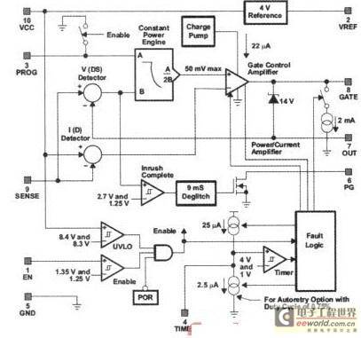
TPS2491 is a positive high-voltage hot-swap controller launched by TI, which supports 9-80 V positive voltage systems and is suitable for protecting emerging positive high-voltage distributed power systems, such as 12 V, 24 V and 48 V server backplanes, storage area networks, medical systems, plug-in modules and wireless base stations. The programmable power and current limit functions of TPS2491 help ensure that the external MOSFET always operates within its safe operating area (SOA) under appropriate voltage, current and time conditions. During normal operation, the external MOSFET can operate at the maximum gate-source voltage to minimize the channel resistance. During startup and short circuit conditions, the gate-source voltage can be modulated to provide a defined startup time to avoid damage to the external MOSFET. The TPS2491 functional block diagram is shown in Figure 2.

Figure 2 TPS2491 functional block diagram
1) Power-on startup process
When the undervoltage lockout (UVLO) and chip enable (EN) both exceed their threshold levels, the GATE, PROG, TIMER and PG pins are set to the active state, the external MOSFET is turned on under the GATE drive, and the controller uses VSENSE-OUT and VVCC-SENSE to monitor the voltage (VDS) and current (ID) from the drain to the source of the MOSFET respectively. [page]
2) Current control and programmable
controller monitors the current ID flowing through the MOSFET through the voltage drop across the external sense resistor Rs. When the surge current occurs, the MOSFET gate voltage is reduced to maintain the voltage drop across the sense resistor at 50 mV to achieve the control of the surge current during hot plugging. The maximum output current is adjusted by changing the value of the sense resistor Rs.
3) MOSFET dissipation power limit
controller determines the maximum allowable dissipation power on the MOSFET through the input voltage of the RPOG pin, that is, VPROG=PLIM/(10*ILIM), and determines the size of the timing capacitor GT in combination with the SOA of the selected external MOSFET to ensure that the MOSFET always operates in its safe operating area.
4) Overload protection
An integral capacitor CT is connected to the TIMER pin to provide overload delay timing and controller restart interval timing. When the power supply voltage drops due to hot plug or output short circuit, CT is charged and TIMER timing starts. At this time, the MOSFET gate drive circuit controls the ID constant current. When CT charges to 4 V, the GATE pin is pulled low and the MOSFET is turned off. Thereafter, the internal circuit controls CT to discharge. When the discharge reaches 1 V, GATE is re-enabled and the controller automatically restarts. Thereafter, if there is still an overload, the above process will be repeated.
2.2 24V protection circuit design
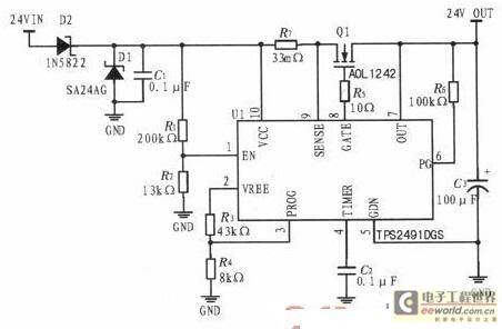
This section introduces the design process of the positive voltage 24 V hot plug circuit in detail based on TPS2491. The circuit schematic is shown in Figure 3. Set VIN (MAX) = 24 V and the maximum output current IMAX = 1.5 A.
1) Selection of the sensing resistor Rs (R7 in Figure 3)

Figure 3 24V hot-swap circuit schematic
Rs=0.05/(1.2×IMAX), value is 33 mΩ, IMAX≈1.5 A.
2) Selection of external MOSFET
The VDS withstand voltage of the external N-channel MOSFET should be greater than the input voltage and transient overshoot, and there should be a certain margin, and RDSON (MAX) should be met, where TJ (MAX) is generally 125℃, and the thermal resistance RθJA depends on the packaging and heat dissipation of the tube. According to the above conditions, the N-channel MOSFET AOLL1242 was selected as the external MOSFET for the 24V hot-swap circuit in the design, with VDS=40V, ID=69A (VGS=10 V), which meets the design requirements of the maximum input voltage of 24 V and the maximum output current of 1.5 A, and leaves enough margin to prevent transient overshoot. 3) MOSFET PLIM setting MOSFET will have a huge power consumption during hot-swap and output short circuit. Limiting PLIM can protect the tube from being damaged by excessive temperature. By adjusting the voltage of the pin PROG, the size of PLIM is set, and the following conditions must be met: 4) Selection of timing capacitor CT (C2 in Figure 3) In addition to completing the setting of the fault restart interval timing, the power dissipation of the external MOSFET during the overload duration timing must also be met, so as not to cause damage to the tube. In the design, CT=0.1μF is selected. 5) Enable startup voltage setting The controller enable startup voltage is 1.35 V, and the shutdown voltage is 1.25 V. By setting the EN pin input voltage, the power input undervoltage protection can be achieved. In the design, R1=200 kΩ and R2=13 kΩ are selected. From the formula VIN(ON)=1.35/[R2/(R1+R2)]=22 V, it can be seen that the controller enables startup when the power input voltage reaches 22 V; from the formula VIN(OFF)=1.25/[R2/(R1+R2)]=20.5 V, it can be seen that the controller enters undervoltage protection when the power input voltage drops to 20.5 V. 6) Other selections In order to suppress high-frequency oscillation, the GATE drive resistor R5 is set to 10Ω; to ensure that the PG pin absorbs less than 2 mA, the pull-up resistor R6 is set to 100 kΩ; C1 is set to 0.1μF, and D1 selects the Zener TVS tube SA24AG; the IN5822 Schottky diode D2 is connected in series to the 24 V power input to prevent reverse power connection.


3 Circuit test verification
The positive voltage 24 V hot-swap protection circuit designed in this article is applied to the data acquisition card with backplane structure for testing and verification. The voltage of the power bus of the acquisition card backplane is 24 V.
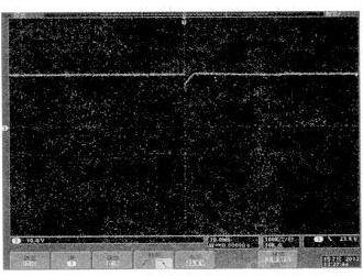
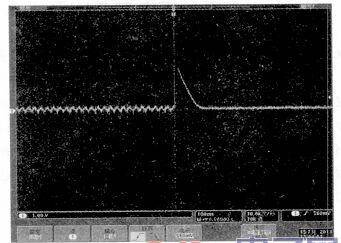
Test method: When the acquisition card is inserted into the backplane, the waveform change of the backplane power bus and the waveform change of the positive electrode of the timing capacitor CT are monitored by an oscilloscope. [page] Test
results: When the data acquisition card has no hot-swap protection circuit, the waveform of the backplane power bus is shown in Figure 4 when the acquisition card is inserted into the backplane; when the data acquisition card has a hot-swap protection circuit, the waveform of the backplane power bus is shown in Figure 5 when the acquisition card is inserted into the backplane, and the waveform of the positive electrode of the timing capacitor CT is shown in Figure 6.

Figure 4 Backplane power bus waveform without hot-swap protection circuitFigure 5 Backplane power bus waveform with hot-swap protection circuitFigure 6 Timing capacitor waveform with hot-swap protection circuit

When the circuit is inserted into the live backplane, the 24 V power bus voltage of the backplane has an instantaneous drop of about 6V (about 3 ms). It can be seen that if the load capacitance is larger, the voltage drop of the backplane power bus will be larger and the drop time will be longer. In such a voltage drop amplitude and time, it is possible to cause other normally working acquisition cards on the backplane to reset, and even damage the interface circuit due to the instantaneous large load capacitance charging surge current.
It can be seen from the waveform in Figure 5 that when the acquisition card has a hot-swap protection circuit, when it is inserted into the live backplane, the 24 V power bus voltage of the backplane has almost no drop. At the same time, from the analysis of Figure 6, it can be seen that when the acquisition card is hot-plugged, a surge overcurrent occurs, and the timing capacitor CT begins to charge. During the charging process, the MOSFET gate drive circuit maintains a constant current output by the power supply. Since the acquisition card load capacitor has been fully charged before CT charging reaches 4 V (about 2 V), the hot-plug controller immediately cancels the current limiting protection and enters the normal working state, controlling CT to start discharging. It can be clearly seen in Figure 6 that the CT charging cycle is much smaller than the discharge cycle, which also verifies the difference between the CT charging current (25μA) and the discharge current (2.5μA).
4 Conclusion
With the continuous improvement of the application requirements of industrial sites, higher requirements are put forward for product design methods. The backplane structure has its inherent flexibility and scalability, and the faulty board can be replaced and plugged in while the system maintains normal operation, which is very suitable for practical application in industrial sites. The surge current generated during the hot-plugging process will not only cause the accidental reset of other normally operating boards in the system, but may even damage the related interface circuits.
This article introduces in detail the process of hot-swap protection circuit design based on TPS2491, and verifies it through the design of 24 V power backplane bus data acquisition card. From the verification results, it can be seen that the hot-swap protection circuit designed in this article effectively suppresses the surge current during the hot-swap process, and the hot-swap circuit works normally and meets the design requirements. Therefore, the hot-swap protection circuit and its design method introduced in this article have high reference value and application value.
Previous article:Design of MRS signal acquisition module based on orthogonal vector amplification ---- Hardware design of acquisition module (Part 3)
Next article:Additional Phase Noise Test Techniques and Test Process Considerations
- Popular Resources
- Popular amplifiers
- From probes to power supplies, Tektronix is leading the way in comprehensive innovation in power electronics testing
- Seizing the Opportunities in the Chinese Application Market: NI's Challenges and Answers
- Tektronix Launches Breakthrough Power Measurement Tools to Accelerate Innovation as Global Electrification Accelerates
- Not all oscilloscopes are created equal: Why ADCs and low noise floor matter
- Enable TekHSI high-speed interface function to accelerate the remote transmission of waveform data
- How to measure the quality of soft start thyristor
- How to use a multimeter to judge whether a soft starter is good or bad
- What are the advantages and disadvantages of non-contact temperature sensors?
- In what situations are non-contact temperature sensors widely used?
- LED chemical incompatibility test to see which chemicals LEDs can be used with
- Application of ARM9 hardware coprocessor on WinCE embedded motherboard
- What are the key points for selecting rotor flowmeter?
- LM317 high power charger circuit
- A brief analysis of Embest's application and development of embedded medical devices
- Single-phase RC protection circuit
- stm32 PVD programmable voltage monitor
- Introduction and measurement of edge trigger and level trigger of 51 single chip microcomputer
- Improved design of Linux system software shell protection technology
- What to do if the ABB robot protection device stops
- Analysis of the application of several common contact parts in high-voltage connectors of new energy vehicles
- Wiring harness durability test and contact voltage drop test method
- From probes to power supplies, Tektronix is leading the way in comprehensive innovation in power electronics testing
- From probes to power supplies, Tektronix is leading the way in comprehensive innovation in power electronics testing
- Sn-doped CuO nanostructure-based ethanol gas sensor for real-time drunk driving detection in vehicles
- Design considerations for automotive battery wiring harness
- Do you know all the various motors commonly used in automotive electronics?
- What are the functions of the Internet of Vehicles? What are the uses and benefits of the Internet of Vehicles?
- Power Inverter - A critical safety system for electric vehicles
- Analysis of the information security mechanism of AUTOSAR, the automotive embedded software framework
- Questions about the power supply of the communication system
- [Shanghai Hangxin ACM32F070 development board] The second part lights up the LCD screen and operates the touch button functions, serial port, ADC.
- EEWORLD University ---- TE Smart City
- Develop IoT in 10 minutes - Smoke sensor monitoring (Wifi version)
- Hearing aid chips
- IMX6 MfgTool Guide
- EEWORLD University Hall----Automatic Control System (Henan Polytechnic University)
- TI's AWR1243 radar learning record
- Help max30001 FIFO ECG
- RIGOL FPGA Technology Talent Recruitment Call


 ISL28414FBZ-T7


 京公网安备 11010802033920号