The technical indicators of the high-speed data acquisition board in this design are as follows: a) vertical resolution 12 bits; b) dual channels work simultaneously and alternately sample, and the single channel sampling rate is 500MSPS; c) effective resolution is greater than or equal to 10 bits; d) signal-to-noise ratio SNR>62dB. The main components of the acquisition board system are ADC chip, clock chip and analog amplifier and filter on the channel.
Through comprehensive analysis of performance indicators, we choose ADS5463 as our ADC chip and AD9517-3 as the clock chip. The impedance matching problems encountered in the data acquisition board are mainly concentrated on these two chips.
The sampling rate of ADS5463 is 500MSPS, the vertical resolution is 12bits, and the effective resolution is 10.5bits. The input amplitude range of the clock signal of ADS5463 is very wide, and the peak-to-peak value of the input clock signal can reach up to 3 volts. The signal-to-noise ratio of ADS5463 is related to the amplitude of the clock signal, the size of the common-mode voltage, the temperature, and the ripple of the power supply voltage. Among them, the amplitude of the clock signal has a greater impact on the signal-to-noise ratio. The higher the peak-to-peak value of the clock signal, the higher the signal-to-noise ratio. The format of the data output is LVDS level.
AD9517 is a programmable 12-channel clock generator. AD9517 has a built-in 2GHz VCO, which can generate LVDS clock signals up to 800MHz and LVPECL clock signals up to 1.6GHz. By setting the registers, clock output signals of different level standards and frequencies can be generated.
In order to maximize the signal-to-noise ratio of ADS5463, the output clock of AD9517 adopts LVPECL level. The signal swing of LVPECL is 800mV, and the output impedance is very low, so it has strong driving ability. The output of ADS5463 is LVDS level, and the output of AD9517 is LVPECL level, both of which are differential signals. In order to control the impedance of the differential line and find a good termination solution, the definition of differential impedance is introduced below.
Differential Line Impedance
For edge-coupled microstrip lines made of FR4 material, the differential impedance is approximately:
In the formula, Zdiff represents differential impedance in Ω; Z0 represents the single-ended characteristic impedance when uncoupled; s represents the spacing between the edges of the signal line in mil; h represents the dielectric thickness between the signal line and the return path plane; the dielectric constant of FR4 medium determines the two coefficients in the formula, 0.48 and 0.96.
For edge-coupled striplines in FR4 material, the differential impedance is approximately:
In the formula, the dielectric constant of FR4 medium determines the two coefficients 0.37 and 2.9 in the formula, b represents the total dielectric thickness between the planes, and the rest is the same as formula (1).
In a transmission line, the total attenuation caused by the conductor is:
In the formula, Len is the length of the transmission line, in units of in; Z0 is the characteristic impedance of the transmission line, in units of Ω; w is the line width, in units of mil; f is the sine wave frequency component, in units of GHz; Acond is the total attenuation caused by the conductor, in units of dB; 36 This parameter is related to the dielectric dissipation factor tan(δ) of the FR4 medium, which is 0.02. [page]
Impedance matching and termination of transmission lines
In order to make the AD acquisition system meet the design specifications, with the help of HyperLynx simulation software, the board-level simulation of the ADS5463 acquisition system is completed to reduce or even eliminate the ringing caused by impedance mismatch or termination error, so that the AD acquisition system can work normally at the specified frequency (500MHz). The above formulas (1)(2)(3) are used to calculate and analyze the experimental results.
The stacked structure of the signal integrity verification board of the high-speed digital acquisition board is shown in Figure 1.
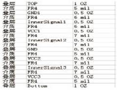
Figure 1. The laminated structure of the verification board
In order to make the multilayer printed circuit board meet the electromagnetic compatibility and sensitivity standards during normal operation, the signal return path and the impedance of the power supply and ground layer should be considered when designing the layering and stacking of the multilayer printed circuit board.
For transmission lines in multilayer boards, the impedance of the driver is mainly determined by the impedance of the signal path and the plane closest to it, and has nothing to do with the plane actually connected to the return end of the driver. For high-speed digital boards, good termination of signal lines becomes very important. We hope that the impedance of the driver can be controlled, so that it is easy to terminate the signal line well during design. In order to meet the requirements of controllable impedance, when designing high-speed digital boards, the wiring layer should be arranged adjacent to the image plane layer, and important signal lines should be close to the ground layer. The image plane layer here refers to the power layer and the ground layer, that is, the return path of the signal should be the power layer or the ground layer. The signal layer InnerSignal1 on the board follows the above design principles. InnerSignal1 is adjacent to the two image plane layers GND1 and VCC1, forming a stripline structure, which is convenient for controlling the characteristic impedance of the transmission line by controlling the thickness of the medium and the width of the trace during design.
In addition to the signal return path, power and ground impedance is also a factor to be considered when layering. In order to reduce ground bounce and track collapse, the inductive impedance between power and ground should be minimized during design. In order to minimize the inductive impedance between power and ground, the power plane and ground plane are required to be adjacent and as close as possible. The core voltage of the FPGA is laid on the VCC2 power layer. The power layer VCC2 and GND layers on the board are adjacent and the dielectric thickness is only 5mil, which will reduce the inductive reactance between VCC2 and GND.
The devices on the verification board are: one AD9517 clock chip is used to provide clock for ADS5463, one ADS5463 is used for data acquisition, two FPGAs are Altera's StratixII series EP2S60 for receiving and processing data collected by AD, and five LT1764 chips are used to provide power on the board.
First, the clock line of ADS5463 is analyzed. In order to make ADS5463 have a higher signal-to-noise ratio, the output clock of AD9517 is set to LVPECL level. The layout of the clock line from AD9517 to ADS5463 on the verification board is shown in Figure 2.
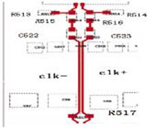
Figure 2 PCB layout of the clock line
The clock signal is terminated in parallel with AC coupling. R517 in Figure 2 is a parallel termination resistor with a resistance of 100Ω. C523 and C522 are AC coupling DC blocking capacitors with a capacitance of 0.1nF. The existence of C523 and C522 will make the clock signal of ADS5463 use the 2.5V reference level of ADS5463 as the common mode voltage. R515 and R516 are zero and do not work in this design. Since the LVPECL output is an emitter-follower output structure, two resistors are required to pull a DC bias voltage. Resistors R513 and R514 are used to provide bias voltage with a resistance of 200Ω. The clock lines clk- and clk+ are laid out on the top layer and are a pair of edge-coupled microstrip lines. The structure of the microstrip lines clk- and clk+ is: s=4mil, h=5mil, Z0=62.72Ω, and the medium is FR4. From formula (1), Zdiff=99.03Ω can be calculated. Obviously, the characteristic impedance of the transmission line and the resistance of the termination resistor R517 are very close, and the clock signal has a very slight reflection. The clock lines clk- and clk+ are simulated using HyperLynx simulation software. The eye diagram of the clock signal received by the clock input end of ADS5463 is shown in Figure 3.
The hexagonal part and the rectangular frame in Figure 3 are the test templates for the eye diagram, and the other parts are the eye diagram of the receiving end. For the LVPECL level, the noise margin is 200mV. The typical value of the output voltage is 800mV, and the maximum threshold voltage is 300mV. The typical value of the rise time and fall time of the ADS5463 is 500ps (Note: The rise time and fall time here refer to the time occupied by the 20% to 80% length of the rising edge and the falling edge). Based on these parameters, we set the template for the eye diagram test. The template for the eye diagram test is the hexagon in Figure 3.
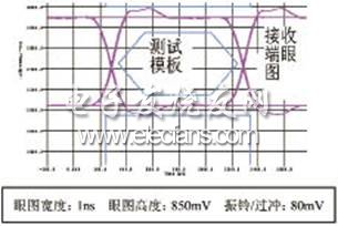
Figure 3 Eye diagram of clock signal
The simulation results show that the width of the eye diagram is 1ns, the height of the eye diagram is about 850mV, the height of the overshoot is about 80mV, and the eye diagram at the receiving end does not touch the template. From the above analysis, the differential clock signal received by ADS5463 meets the LVPECL level standard and can be used in the AD acquisition system. The simulated eye diagram is not perfect. The small amplitude ringing and overshoot generated in the eye diagram are related to the impedance mutation caused by the short stubs at the termination resistor, the DC blocking capacitor, and the resistor that provides the bias voltage. Reducing the length of these short stubs will further improve the quality of the eye diagram.
In addition to the clock line, another important signal line on the board that needs to be simulated is the data line of ADS5463. ADS5463 sends the data after AD conversion to StratixII through a 12-bit data bus for processing. After completing the simulation of the AD clock line, the next step is to simulate the AD data line. The data line layout on the board is shown in Figure 4.
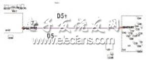
Figure 4 PCB layout of data line
The second group of transmission lines on the verification board are data lines D5+/D5-. This differential line is the data line between ADS5463 and StratixII. ADS5463 is the transmitter and StratixII is the receiver. StratixII provides 100Ω on-chip termination. The data transmission rate is 500MHz, LVDS level. The length of the second group of transmission lines is 2.83in. Most of the transmission lines are on the Signal1 signal layer, and only a very short part is on the top layer. For the D5+ transmission line, the length of the microstrip line on the top layer is 105.86mil (0.10586in), and for the D5- transmission line, the length of the microstrip line on the top layer is 95.07mil (0.09507in). That is, the length of the transmission line with impedance mutation is short enough. Although reflections still occur, these reflections are covered by the rising or falling edge of the signal. The impact of these reflections on the signal integrity of the transmission line can be ignored. The characteristic impedance of the transmission line D5+/D5- is determined by the part on the Signal1 signal layer.
For the stripline of D5+/D5- in the signal layer Signal1, Z0=52.43Ω, b=12mil, s=9mil, and the medium is FR4. According to formula (2), Zdiff=99.13Ω. That is, the differential impedance of the stripline is Zdiff=99.13Ω.
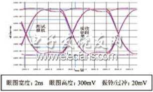
The data lines D5- and D5+ of ADS5463 are simulated using HyperLynx simulation software. The eye diagram of the data signal obtained by the Stratix II at the receiving end is shown in Figure 5.
Previous article:High-speed data transmission interface DDR2 I/F characteristics and testing
Next article:Application of clock distribution chip in high-speed parallel data acquisition
- Keysight Technologies Helps Samsung Electronics Successfully Validate FiRa® 2.0 Safe Distance Measurement Test Case
- From probes to power supplies, Tektronix is leading the way in comprehensive innovation in power electronics testing
- Seizing the Opportunities in the Chinese Application Market: NI's Challenges and Answers
- Tektronix Launches Breakthrough Power Measurement Tools to Accelerate Innovation as Global Electrification Accelerates
- Not all oscilloscopes are created equal: Why ADCs and low noise floor matter
- Enable TekHSI high-speed interface function to accelerate the remote transmission of waveform data
- How to measure the quality of soft start thyristor
- How to use a multimeter to judge whether a soft starter is good or bad
- What are the advantages and disadvantages of non-contact temperature sensors?
- Innolux's intelligent steer-by-wire solution makes cars smarter and safer
- 8051 MCU - Parity Check
- How to efficiently balance the sensitivity of tactile sensing interfaces
- What should I do if the servo motor shakes? What causes the servo motor to shake quickly?
- 【Brushless Motor】Analysis of three-phase BLDC motor and sharing of two popular development boards
- Midea Industrial Technology's subsidiaries Clou Electronics and Hekang New Energy jointly appeared at the Munich Battery Energy Storage Exhibition and Solar Energy Exhibition
- Guoxin Sichen | Application of ferroelectric memory PB85RS2MC in power battery management, with a capacity of 2M
- Analysis of common faults of frequency converter
- In a head-on competition with Qualcomm, what kind of cockpit products has Intel come up with?
- Dalian Rongke's all-vanadium liquid flow battery energy storage equipment industrialization project has entered the sprint stage before production
- Allegro MicroSystems Introduces Advanced Magnetic and Inductive Position Sensing Solutions at Electronica 2024
- Car key in the left hand, liveness detection radar in the right hand, UWB is imperative for cars!
- After a decade of rapid development, domestic CIS has entered the market
- Aegis Dagger Battery + Thor EM-i Super Hybrid, Geely New Energy has thrown out two "king bombs"
- A brief discussion on functional safety - fault, error, and failure
- In the smart car 2.0 cycle, these core industry chains are facing major opportunities!
- The United States and Japan are developing new batteries. CATL faces challenges? How should China's new energy battery industry respond?
- Murata launches high-precision 6-axis inertial sensor for automobiles
- Ford patents pre-charge alarm to help save costs and respond to emergencies
- New real-time microcontroller system from Texas Instruments enables smarter processing in automotive and industrial applications
- Which of the two ways of making differential lines of equal length internally is better?
- X-NUCLEO-IKS01A3 Review——by dcexpert
- Can anyone explain this circuit?
- Wireless communication signal propagation
- The 5 yuan proofing board is back
- About the history, reasons and principles of PFC power factor correction
- A highlight of UCOS compared with ordinary mission structures!!
- Implementation of the sharpening algorithm on DSP
- [NXP Rapid IoT Review] Rapid IoT Studio with Examples
- What does IAR do before main?

 Hyperlynx Simulation Tutorial


 京公网安备 11010802033920号