TMS320F2812 is a 32-bit high-performance digital signal processor (DSP) with a main frequency of up to 150 MHz, and an ADC conversion module is integrated inside. The ADC module is a 12-bit, pipelined analog-to-digital converter with a built-in dual sample-and-hold (S/H) and can select 16 channel inputs in multiple ways. The fast conversion time runs at 25 MHz, ADC clock or 12.5 Msps, and the 16 conversion result registers can work in continuous automatic sequencing mode or start/stop mode.
In modern electronic systems, as a key component of the interface between analog systems and digital systems, the analog-to-digital converter (ADC) has become a very important circuit unit for data acquisition in control loops. In actual use, it is found that the conversion result of the ADC has a large error. If this conversion result is directly used in the control loop, the control accuracy will inevitably be reduced. In order to overcome this shortcoming and improve its conversion accuracy, the author proposed a method for improving the accuracy of TMS320F2812 ADC after conducting a large number of experiments, so that the ADC accuracy is effectively improved.
1 Definition and impact analysis of ADC module error
1.1 Error definition
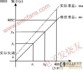
Commonly used A/D converters mainly have: offset error, gain error and linear error. Here we mainly discuss offset error and gain error. Ideally, the conversion equation of the ADC module is y=x×mi, where x=input count value=input voltage×4095/3; y=output count value. In practice, various errors of the A/D conversion module are inevitable. Here, the conversion equation of the ADC module with gain error and offset error is defined as y=x×ma±b, where ma is the actual gain and b is the offset error. After multiple measurements of the ADC signal acquisition of F2812, it is found that the ADC gain error is generally within 5%, that is, 0.95

Figure 1 Ideal ADC conversion and actual ADC conversion
1.2 Impact analysis
In computer measurement and control systems, the acquisition of object data generally includes two basic physical quantities: analog quantity and digital quantity. Computers can read digital quantities directly, but analog quantities can only be accepted by computers after being converted into digital quantities. Therefore, in order to accurately collect and process analog quantities, the precision and accuracy of analog-to-digital conversion must meet certain requirements. Since the ADC of F2812 has a certain gain error and offset error, it is easy to cause system misoperation. The following analyzes the impact of the two errors on linear voltage input and A/D conversion results.
The ADC module input analog voltage provided in the F2812 user manual is 0~3 V, but in actual use, due to the existence of gain error and offset error, its linear input is reduced, as shown in Table 1.

The following takes y=x×1.05+80 as an example to introduce the calculation of various values. When the input is 0, the output is 80. Since the maximum output value of the ADC is 4095, the maximum input voltage value is 2.8013 obtained by the formula y=x×1.05+80. Therefore, the AC input voltage range is 1.4007±1.4007, at which time the effective number of bits N=ln4015/ln2=11.971, mV/count bit=2.8013/4015=0.6977, and the calculation of the remaining items is the same as above. The last row in Table 1 shows the safety parameters of the ADC operation, where the effective number of bits is reduced to 11.865 bits, and mV/count bit is increased from 0.7326 to 0.7345, which will reduce the conversion result by 0.2%.
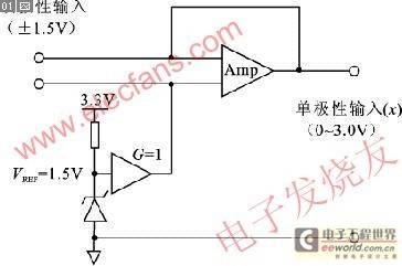
In practical applications, the collected signals are often bipolar signals, so a conversion circuit needs to be added before the signal is sent to the ADC to convert the bipolar signal into a unipolar signal. The typical conversion circuit is shown in Figure 2. For the ADC module, considering the influence of gain error and offset error on the input range, the conversion circuit needs to be adjusted to the circuit shown in Figure 3. In Figure 3, the reference range of the input gain error has been changed.
For bipolar input, the gain error of its 0 V input corresponds to the gain error of 1.4315 V for unipolar input. Therefore, the gain error and offset error of the original ADC are increased. For example, if the gain error of the ADC is 5% and the offset error is 2%, then the bipolar gain error is calculated as follows: bipolar input x′= 0.0000 V, unipolar ADC input voltage x = 1.4315 V, its ideal conversion value is ye=1.4315×4095/3=1954, and the actual conversion value is calculated by ya=1954×1.05+80, then the bipolar gain error is ya-ye=2132-1954=178 (9.1% error). It can be seen from the calculation that the error of the ADC is greatly increased. Therefore, if you want to use the ADC for data acquisition, you must calibrate the ADC to improve its conversion accuracy.

Figure 2 Ideal voltage conversion circuit
 [page]
Figure 3 Corrected voltage conversion circuit
2 ADC correction
2.1 Correction method
From the above analysis, it can be seen that the main reason for the poor ADC conversion accuracy of F2812 is the existence of gain error and offset error. Therefore, to improve the conversion accuracy, the two errors must be compensated. The following method is adopted to correct the ADC module.
Select any two channels of the ADC as reference input channels, and provide them with known DC reference voltages as inputs (the two voltages cannot be the same). Obtain the conversion value by reading the corresponding result register, and use the two sets of input and output values to obtain the correction gain and correction offset of the ADC module. Then use these two values to compensate for the conversion data of other channels, thereby improving the conversion accuracy of the ADC module. Figure 1 shows how to use the equation to obtain the correction gain and correction offset of the ADC. The specific calculation process is as follows:
① Obtain the conversion values yL and yh of the known input reference voltage signal.
② Use the equation y=x×ma+b and the known reference values (xL, yL) and (xH, yH) to calculate the actual gain and offset errors:
actual gain ma=(yH-yL)/(xH-xL);
offset error b="yL" -xL×ma.
③ Define the input x=y×CalGain-CalOffset, then the equation y=x×ma+b gives the correction gain CalGain=1/ma=(xH-xL)/(yH -yL), and the correction offset CalOffset=b/ma=yL/ma-xL.
④ Apply the required correction gain and correction offset to other measurement channels to correct the ADC conversion results.
The above is the whole process of realizing ADC correction. By using this method, the conversion accuracy of ADC is greatly improved. Since this method uses the error of a certain channel to correct the error of other channels, to use this method, it is necessary to ensure that the channel error between channels is small. For the F2812ADC conversion module, since the gain and offset errors between its channels are within 0.2%, this method can be used to calibrate it.
2.2 Software Implementation
Compared with the general ADC conversion program, the ADC conversion program with correction needs to add two additional program segments: calculation of the correction value and processing of the ADC using the correction value. In order to facilitate operation and obtain conversion results, the structure variable ADCCALIBRATIONVARS is defined in the implementation to save various data after ADC conversion. In addition, to improve the versatility of the program, the sampling method, reference voltage value and ideal conversion values of high and low voltages are all defined in the ADC conversion header file ADCCalibration.h. ADCCALIBRATIONVARS is defined as follows:
typedefstruct{
Uint*RefHighChAddr;//reference high voltage connected channel address
Uint*RefHighChAddr;//reference low voltage connected channel address
Uint*ChoAddr;//0 channel address
UintAvg_RefHighActualCount;//reference high voltage actual conversion value
UintAvg_RefHighActualCount;//reference low voltage actual conversion value
UintRefHighIdealCount;//reference high voltage ideal conversion value
UintRefLowCount;//reference low voltage actual conversion value
UintCalGain;//calibration gain
UintCalOffset;//calibration offset
//calibration channel conversion value
UintCh0;
UintCh16;
}ADC CALIBRATION VARS;
The entire A/D conversion task consists of the interrupt function intADC() and the main function ADCCalibration(). The interrupt function is mainly used to read the conversion data, while the calibration parameter calculation and the correction of the conversion results of each channel are completed in the main function. After the correction, the result is saved in the defined structure variable. Here, the ADC is corrected using a single-sample single-correction processing method. Of course, a multi-sample single-correction processing method can also be used. However, in order to improve the accuracy, if the design system cost allows, it is recommended to use a single-sample single-correction method to improve the ADC accuracy.
2.3 Experimental results
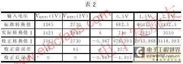
The author conducted experiments on the F2812 system he used, using 1 V and 2 V as reference voltages, and channels A6 and A7 as reference channels. By comparing the data before and after the correction of 0 V, 0.5 V, 1.5 V, and 2.5 V, it was found that after using the above correction method, the conversion accuracy of the ADC was significantly improved. The comparison results are listed in Table 2.

Note: Calculated from the reference voltage: CalGain=0.965; CalOffset=6.757.
The data given in Table 2 are only a set of data obtained by the author after a large number of experiments. The experiments prove that the error of ADC can be controlled within 0.5% after correction, which meets the requirements for most measurement and control systems. For systems with higher conversion accuracy requirements, an external A/D converter can be used.
Conclusion
The A/D converter is the core component of the data acquisition circuit. Its good precision and accuracy are the key to improving the performance of the data acquisition circuit. TMS320F2812, a 32-bit processor integrating microcontroller and digital signal processor launched by TI, is widely used for its high running speed and powerful processing functions. The improvement of the accuracy of its ADC module will further improve its application in the control field. The correction algorithm proposed in this paper to improve the accuracy of the ADC module has been proven to be practical and feasible in actual application.
Previous article:Challenges and suggestions for DDR signal measurement methods and signal integrity verification
Next article:Digital multimeter maintenance methods and techniques
Recommended ReadingLatest update time:2024-11-16 21:45

- Popular Resources
- Popular amplifiers
- Keysight Technologies Helps Samsung Electronics Successfully Validate FiRa® 2.0 Safe Distance Measurement Test Case
- From probes to power supplies, Tektronix is leading the way in comprehensive innovation in power electronics testing
- Seizing the Opportunities in the Chinese Application Market: NI's Challenges and Answers
- Tektronix Launches Breakthrough Power Measurement Tools to Accelerate Innovation as Global Electrification Accelerates
- Not all oscilloscopes are created equal: Why ADCs and low noise floor matter
- Enable TekHSI high-speed interface function to accelerate the remote transmission of waveform data
- How to measure the quality of soft start thyristor
- How to use a multimeter to judge whether a soft starter is good or bad
- What are the advantages and disadvantages of non-contact temperature sensors?
- Innolux's intelligent steer-by-wire solution makes cars smarter and safer
- 8051 MCU - Parity Check
- How to efficiently balance the sensitivity of tactile sensing interfaces
- What should I do if the servo motor shakes? What causes the servo motor to shake quickly?
- 【Brushless Motor】Analysis of three-phase BLDC motor and sharing of two popular development boards
- Midea Industrial Technology's subsidiaries Clou Electronics and Hekang New Energy jointly appeared at the Munich Battery Energy Storage Exhibition and Solar Energy Exhibition
- Guoxin Sichen | Application of ferroelectric memory PB85RS2MC in power battery management, with a capacity of 2M
- Analysis of common faults of frequency converter
- In a head-on competition with Qualcomm, what kind of cockpit products has Intel come up with?
- Dalian Rongke's all-vanadium liquid flow battery energy storage equipment industrialization project has entered the sprint stage before production
- Allegro MicroSystems Introduces Advanced Magnetic and Inductive Position Sensing Solutions at Electronica 2024
- Car key in the left hand, liveness detection radar in the right hand, UWB is imperative for cars!
- After a decade of rapid development, domestic CIS has entered the market
- Aegis Dagger Battery + Thor EM-i Super Hybrid, Geely New Energy has thrown out two "king bombs"
- A brief discussion on functional safety - fault, error, and failure
- In the smart car 2.0 cycle, these core industry chains are facing major opportunities!
- The United States and Japan are developing new batteries. CATL faces challenges? How should China's new energy battery industry respond?
- Murata launches high-precision 6-axis inertial sensor for automobiles
- Ford patents pre-charge alarm to help save costs and respond to emergencies
- New real-time microcontroller system from Texas Instruments enables smarter processing in automotive and industrial applications
- Let’s talk about the key points of the four technical solutions for wireless charging technology
- From basics to theory and application: Spectrum View, a powerful frequency domain analysis tool on an oscilloscope
- Thank you EEWORLD, I received the gift^_^
- Looking for power amplifier solution
- Record power-on time and power-off time
- Detailed explanation of UART serial port protocol
- Why does the phone's battery drain too quickly after it is connected to a Bluetooth device?
- RVB2601 Recording and Playback
- EEWORLD University ---- VLSI CADII-Design
- A comprehensive vocabulary handbook on embedded systems

 Vehicle Electronic Control Technology 2018 Edition


 京公网安备 11010802033920号