Detailed explanation of 5v charger circuit diagram
Source: InternetPublisher:smallembedded Keywords: Charger circuit Updated: 2024/08/23
Working principle of 5V charger
First, the 220V AC power is half-wave rectified by D1 and filtered by C2 before being fed to the load-related circuit. C2 is a filter and R3 is a short-circuit protection. When the load is overcurrent, R3 automatically burns out, thus achieving protection without affecting the operation of the previous circuit.

2. The filtered voltage provides a positive bias voltage to the base of Q1 through the R1 startup resistor. In addition, the filtered voltage provides a bias voltage to the collector of Q1 through the L1 voltage. At this time, Q1 starts to conduct, and R2/C1/D2 acts as a spike absorber and works when Q1 is cut off.
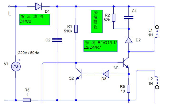
3. When the transistor Q1 starts to turn on, the collector current starts to increase from 0. At this time, current is generated in the collector, and an induced electromotive force of up+down- will be generated at both ends of L1. The small circle represents the same-named end. When L1 is up+down-, both ends of L2 are also up+down-, and then added to the base of Q1 through C3/R6. In this way, Q1 quickly goes from conduction to amplification and then to saturation. When Q1 is saturated, the collector current will no longer increase, and Q1 will retreat from saturation to the amplification area. At this time, the induced electromotive force at both ends of L1 will change from up-down+, and L2 will also change from up-down+. At this time, when the voltage of L2 down+ is adjusted to 5.1V, D4 will be broken down. At this time, D4 will stabilize to a voltage of 5.1V, thereby turning on Q2. When Q2 is turned on, the base potential of Q1 will be pulled down, and Q1 will be cut off immediately.
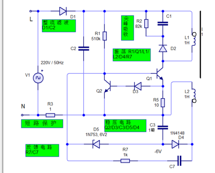
4. When the first cycle of Q1 ends, the starting resistor R1 provides a forward voltage for a new round of conduction, thereby repeatedly opening and closing. When L1 is up+ and down-, L3 is up-down+. At this time, D6 is not conducting and the load has no voltage output. When the induced electromotive force of L1 becomes up-down+, L3 will become up+down-. At this time, D6 is turned on and a 5V voltage output is obtained after filtering by C4. Similarly, the indicator circuit D7 will light up.
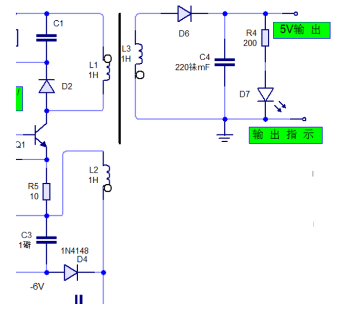
5v charger circuit diagram (I)
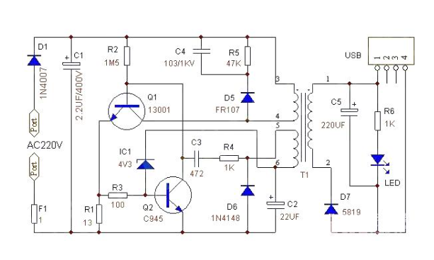
5v charger circuit diagram (II)
a. According to the material: silicon tube, germanium tube b. According to the structure: npn, pnpc. According to the function: switch tube, power tube, Darlington tube, photosensitive tube, voltage regulator tube, etc. d. According to power: low-power tube, medium-power tube, high-power tube e. According to operating frequency: low-frequency tube, high-frequency tube, overclocking tube f. According to installation method: plug-in transistor, SMD transistor Plug-in transistor The transistors we commonly use: 8050, A733 (massage belt motherboard) SMD 5C (BC807), 6C (BC817), B772, B882, etc. 78l0579l05 three-terminal integrated voltage regulator (internal thermal overload protection, short-circuit current limiting) 78 series is positive voltage output, 79 series is negative voltage output, 05 indicates that the output voltage is 5 volts l indicates that the maximum output current is 100 mA, n=300ma, m=500ma, no letter=1.5a, there are also t, h, p, but they are less used, represented by 3a, 5a and 10a respectively. When the voltage applied to the transistor emitter junction is greater than the conduction voltage of the pn junction, and when the base current increases to a certain extent, the collector current no longer increases with the increase of the base current, but remains near a certain value and does not change much. At this time, the transistor loses its current amplification function, and the voltage between the collector and the emitter is very small. The voltage between the collector and the emitter is equivalent to the on-state of the switch, that is, the on-state of the transistor. The (9) pin of the strs6709 is the voltage control input terminal, and ic602 is the error sampling amplifier. When the 140v main power supply voltage rises, the input voltage of ic602 rises, the output voltage drops, and the current flowing through the light-emitting diode in the optocoupler ic603 increases, which increases the current of the phototransistor in ic602, reduces the ce junction resistance of the phototransistor, and increases the voltage of the (7) pin of the strs6709, controls the internal switch tube to reduce the on-time, and promotes the switch pulse duty cycle to decrease, and the 140v DC voltage decreases until it stabilizes.
该电磁炉mcu智能控制电路的供电电路为低压整流滤波电路中的dc 5 v稳压电路,如图2-15所示,该电路由降压变压器变压器将ac 220v电压将为10-20v的交流低压,由降压变压器的次级绕组输出ac 12v电压,由整流二极管变成直流电压,再经5v三端稳压器进行稳压,输出稳定的dc 5 v电压。整流可采用倍压整流,也可用桥式整流。如果变压器输出电压较低,可以用倍压提高电压。 如果变压器输出电压较高则用桥式整流。低频机的整流可用普通二极管,高频机则用肖特基二极管。储能电容可选用无极性电容,也可以选用电解电容。表1 四种逆变电路拓扑结构的比较电路参数 单端式 推免式 半桥式 全桥式 功率开关管集射极间施加电压 截止二极管箝位 稳态为2e,漏感引起的尖峰使 稳态为e,二极管箝位 稳态为e,二极管箝位 输出相同功率时集电极电流 2 2 功率开关管数量 2 2 2 4 输出滤波电容数量 1 1 2 1 输出容量 中、小 大 中等 大3.2.2振荡逆变电路的设计振荡逆变电路是由脉冲变压器组成,如图所示。
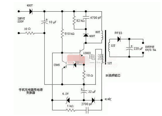
The 1KΩ resistor and the 2700pF capacitor in series at the bottom are the positive feedback branch, which takes the induced voltage from the sampling winding and adds it to the base of the switch tube to maintain oscillation. There is not much to say about the secondary winding on the right. It outputs a 6V voltage after being rectified by the diode RF93 and filtered by the 220uF capacitor. I didn't find any information about the diode RF93, but it is probably a fast recovery tube, such as a Schottky diode. Because the operating frequency of the switching power supply is relatively high, a diode with an operating frequency is required. Common Schottky diodes such as 1N5816 and 1N5817 can be used here instead.
However, since high-frequency and high-voltage transformers are high-frequency and high-voltage, new technical difficulties have emerged: ① As the volume of high-frequency and high-voltage transformers decreases, the frequency increases, the distributed capacitance decreases, and the insulation problem becomes particularly prominent. In particular, high-voltage electrolytic capacitors, high-reverse-voltage high-power switching tubes, and magnetic materials of switching transformers in high-frequency switching power supplies without industrial frequency transformers are still in the research and development stage in my country. 1.2 High-frequency switching AC voltage regulator High-frequency switching AC voltage regulator introduces advanced high-frequency switching power supply technology into AC voltage regulators, thereby reducing the volume and weight, and has the advantages of high efficiency and fast response speed [4].
- Analysis of the working principle of switching regulator
- Build a simple buck-boost regulator and test it on a breadboard
- Schematic diagram of car cigarette lighter to USB power port
- Fabrication of multi-cell lithium battery charging circuit
- Practical and convenient fax machine power supply control circuit
- Isolated two-wire current loop circuit (XTR101, ISO100)
- Simple and practical LED lamp driving circuit
- Offline 8w LED Flyback Power Supply with PFC using NCP1014
- USB power socket using the car battery
- Homemade Electric Bike Fast Charger
- Shandong GD36 charger circuit
- Charger circuit
- Backup power automatic charger circuit
- Charger circuit designed by lm358
- Use BA3105 to make program-controlled charger circuit
- Intelligent battery fast charger circuit 01
- Battery dual constant current charger circuit
- Universal battery charger circuit (2)
- Nickel cadmium battery fast charger circuit
- 6V charger circuit with current limiting


 京公网安备 11010802033920号