Build a simple buck-boost regulator and test it on a breadboard
Source: InternetPublisher:toothache Keywords: Converter Converter Circuit Buck-Boost Regulator Updated: 2024/12/24
Buck-boost regulator is made using two different topologies and as the name suggests it consists of a buck and a boost topology. We already know that the buck regulator topology provides an output voltage with a magnitude lower than the input voltage, whereas the boost regulator topology provides an output voltage with a magnitude higher than the input voltage provided.
For example, if your device is powered by a lithium battery, then the input voltage range will be between 3.6V to 4.2V. If this device requires two operating voltages 3.3V and 5V. Then you need to design a buck-boost regulator to regulate the voltage of the lithium battery to 3.3V and 5V. So, in this tutorial, we will learn how to build a simple buck-boost regulator and test it on a breadboard for easy construction. This regulator is designed to work with a 9V battery and can provide a wide output voltage from 3.3V to 12V with a maximum output current of 4A.
Required Components
XL6009
10k Preset
33uH Inductor - 2pcs
1n4007 - 2 pcs
SR160 - 1 (max 800mA output)
10uH Inductor
100uF capacitor
1000uF capacitor - 2 pcs
1uF ceramic or polyester film capacitor
9V power supply (battery or adapter)
Breadboard
Wires for the breadboard.
XL6009 Buck-Boost Regulator IC
There are many ways to build a buck-boost circuit, for the sake of this tutorial we will use the well-known XL6009 DC/DC converter IC. We chose this IC because it is easy to use and beginner-friendly. You can also check out our article on how to choose a switching regulator IC to help you choose other regulators for your switching design.
The main component is the switching regulator XL6009. The pinout and specifications of XL6009 are shown in the figure below.

The metal sheet is internally connected to the Switching pin of the XL6009 driver ic. The pin description is also given in the table above. The important technical specifications of the XL6009 IC are as follows
feature
5V to 32V wide input voltage range
Positive or negative output voltage programming using a single feedback pin
Current mode control provides excellent transient response
1.25V reference adjustable version
Fixed 400KHz switching frequency
Maximum 4A switching current
SW PIN built-in overvoltage protection
Excellent line and load regulation
EN PIN TTL shutdown capability
Internal optimized power MOSFET
Efficiency up to 94%
Built-in frequency compensation
Built-in soft start function
Built-in thermal shutdown function
Built-in current limiting function
Available in TO263-5L package
The above specification table shows that the minimum input voltage of this driver IC is 5V and the maximum is 32 V. In addition, since the switching frequency is 400 kHz, a smaller inductor can be used for switching related purposes. In addition, the driver IC supports a maximum output current of 4A, which can well cover many high rated current related applications.
Buck-Boost Converter Circuit Using XL6009
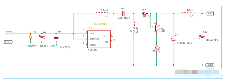
The complete buck-boost converter circuit diagram is shown in the figure below.

For any switching regulator, the inductor and capacitor are the main components. The position of the inductor and capacitor in the circuit is very important to provide the required power to the load during the switching state. In this case, two inductors (L1 and L4) are used, which will support the buck and boost functions respectively in this switching circuit. The 33uH inductor of L1 is the inductor responsible for the buck mode operation, while inductor L2 is used for the boost mode inductor. Here, I have wound my own inductor using a ferrite core and enameled copper wire. If you are not familiar with making your own inductors, you can check out this article on the basics of inductor and inductor coil design to get started. After building the inductor, you can check its value using an LCD meter or if you do not have an LCR meter, you can use an oscilloscope to find the inductor value using the resonant frequency method.
Input capacitors C1 and C2 are used to filter transients and ripples from the external battery or power supply. Capacitor C3, 1uF, 100V is used to isolate the two inductors. There is a Schottky diode SR160, which is a 60V 1 amp diode, used to convert the switching frequency cycle to DC, and capacitor 1000uF, 35V is a filter capacitor used to filter the output of the diode.
Since the feedback threshold voltage is 1.25V, the actual output can be configured by setting the voltage divider based on this feedback voltage. For our circuit, we used a potentiometer (R1) and a resistor (R2) to provide the feedback voltage.
R1 is a variable resistor used to set the output voltage. R1 and R2 form a voltage divider to provide feedback to the driver IC XL6009. 10uH inductor L4 and 100uF capacitor C3 are used as LC filter.
Buck-Boost Converter Structure and Operation
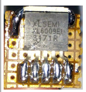
All the components should be easily available except the inductor. The XL6009 IC is not breadboard friendly. Therefore, I used a dotted board to connect the pins of the XL6009 to the male header pins as shown below.

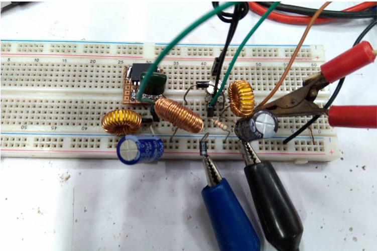
Build the inductor as before and create the circuit. I used a breadboard to keep things simple but a perf board is recommended. Once completed my circuit on the breadboard looked like this.

When the input voltage is higher than the set output voltage, the inductor charges and resists any changes in the current path. When the switch is off, the inductor provides charging current through capacitor C3, which is finally rectified and smoothed by the Schottky diode and capacitor C4 respectively. The driver checks the output voltage through a voltage divider and skips switching cycles based on the feedback circuit output to synchronize the output voltage.
The same thing happens in boost mode when the input voltage is lower than the output voltage and inductor L2 charges and supplies the load current in the off condition.
XL6009 Buck-Boost Converter Circuit Test
This circuit was tested on a breadboard. Please note that we built the circuit on a breadboard for testing purposes only and should not exceed 1.5A when loading the circuit on the breadboard. For higher current applications, it is highly recommended to solder your circuit on a perfboard.
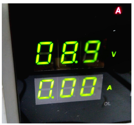
To power the circuit, you can use a 9V battery, but I used a bench power supply set to 9V.

The output voltage can be set from 3.3V to 12V using the potentiometer. Technically, the circuit can be designed for high output currents up to 4A. However, the circuit was not tested at full load due to the limitation of the output diode. The output load was set to a current value of approximately 700-800mA. If necessary, you can change the output diode to increase the output current.
To test our power supply circuit we used a multimeter to monitor the output voltage and for the load we used a DC electronic load similar to the one we built previously. If you don't have an electronic load you can use any load of your choice and monitor the current with a multimeter. A full test video is available at the bottom of this page.
It is also noticed that the output voltage fluctuates within +/-5%. This is due to the high DCR value of the inductor and unavailability of heat sink in XL6009. Adequate heat sink and proper components are useful for a stable output. Overall, the circuit works well and the performance is satisfactory.
- Benefits of Wide Bandgap Technology for Power Converters
- How to use a simple circuit to achieve a smooth soft-start for an isolated converter
- Recommended circuits for different power on times of LM4911
- Single-power supply circuit for ISO122P/ISO124
- Use pulse width modulation to get a precise output voltage
- LED rechargeable flashlight circuit diagram
- Switching power supply circuit composition and function introduction of each part
- LM317 regulated power supply
- Homemade home inverter circuit diagram
- Battery powered switching circuit diagram
- Importance of Voltage Supervisors and Output Topology Selection
- 3v to 5v circuit diagram
- High current (4A) switching regulator integrated circuit L296 outputs 5.1 to 40V
- 3-phase CPU power circuit using HIP6301 and HIP6601 chips
- Warm current power circuit a
- Household emergency power circuit
- Antenna amplifier synchronous power supply circuit
- Wide input 350mA LED driver circuit based on NCL30000
- Telephone power circuit
- 5V, 7.5V, 48V power circuit


 京公网安备 11010802033920号