1. Name of the contestant: Cheng Renjie, Wang Hui
2. Name of the entry: STM32/STM8 Offline Downloader
3. Briefly describe your idea and work:
In current embedded development, STM32 and STM8 are the main control chips used by most engineers. The traditional method is to download the program through a computer and an emulator, and a computer must be configured for production. However, for some mass production, it is obviously appropriate to use a computer, which increases the workload and requires certain professional knowledge. When handing over the production files to the production personnel, it is very likely to cause leakage and huge losses. The offline downloader is small in size and cheap in price. It can set the number of productions and configure encryption in the program, which can effectively protect the production data. At the same time, the offline downloader is easy to operate. As long as the engineer configures it on the computer, he can hand it over to the production personnel with confidence.
4. The materials to be used in the LiChuang Mall: STM32, STM8, W25Q64, buffer, power supply, resistor and capacitor.
5. Intended non-LiChuang Mall materials or other supplements: TFT, shell
6. Intended EDA tool software names: Keil, VS2017, LiChuang EDA design tool
7. Original link: http://club.szlcsc.com/article/details_12812_1.html
8. Original project link: https://oshwhub.com/lengyu1226/wang1111
I. Introduction to the work
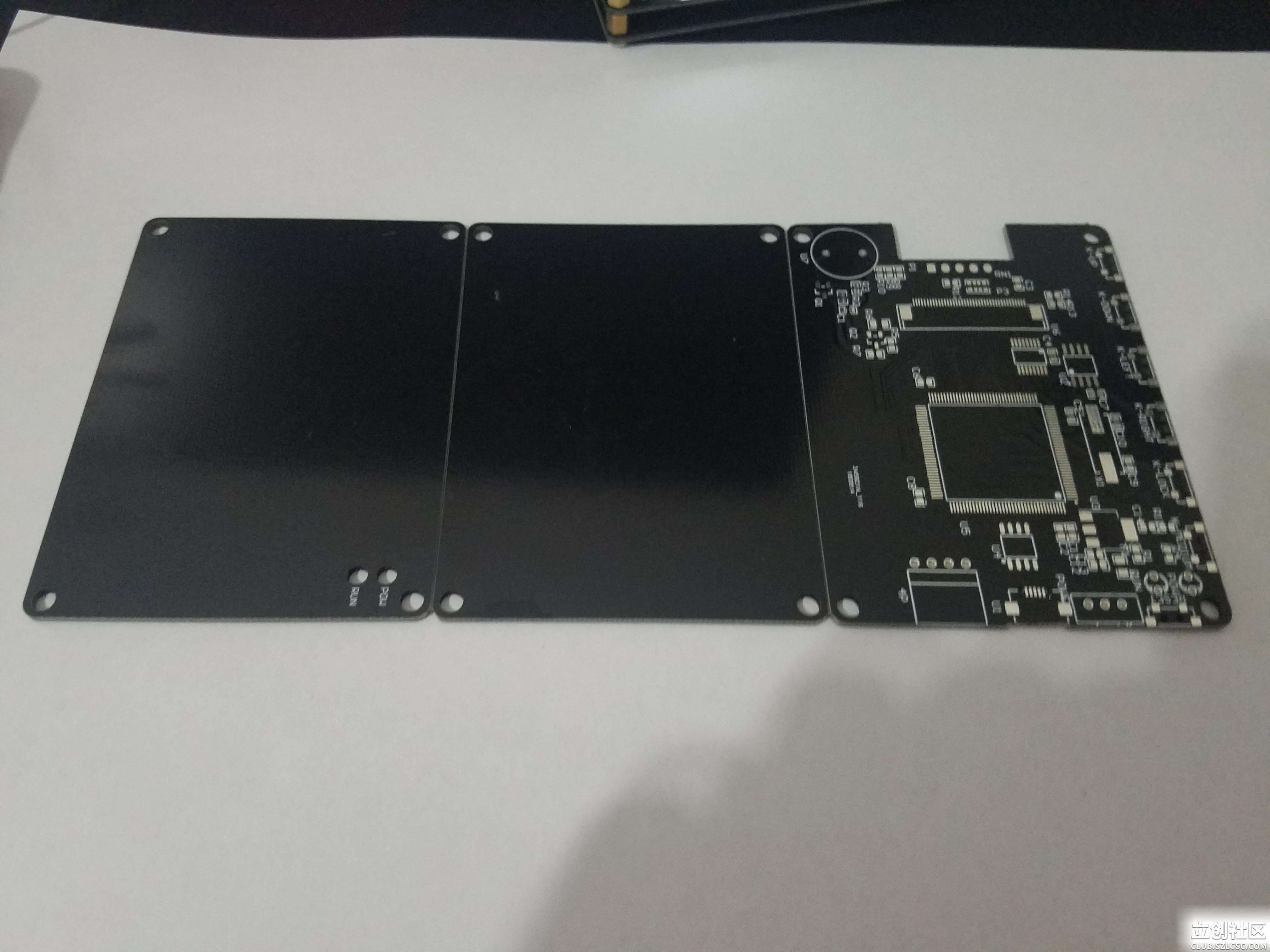
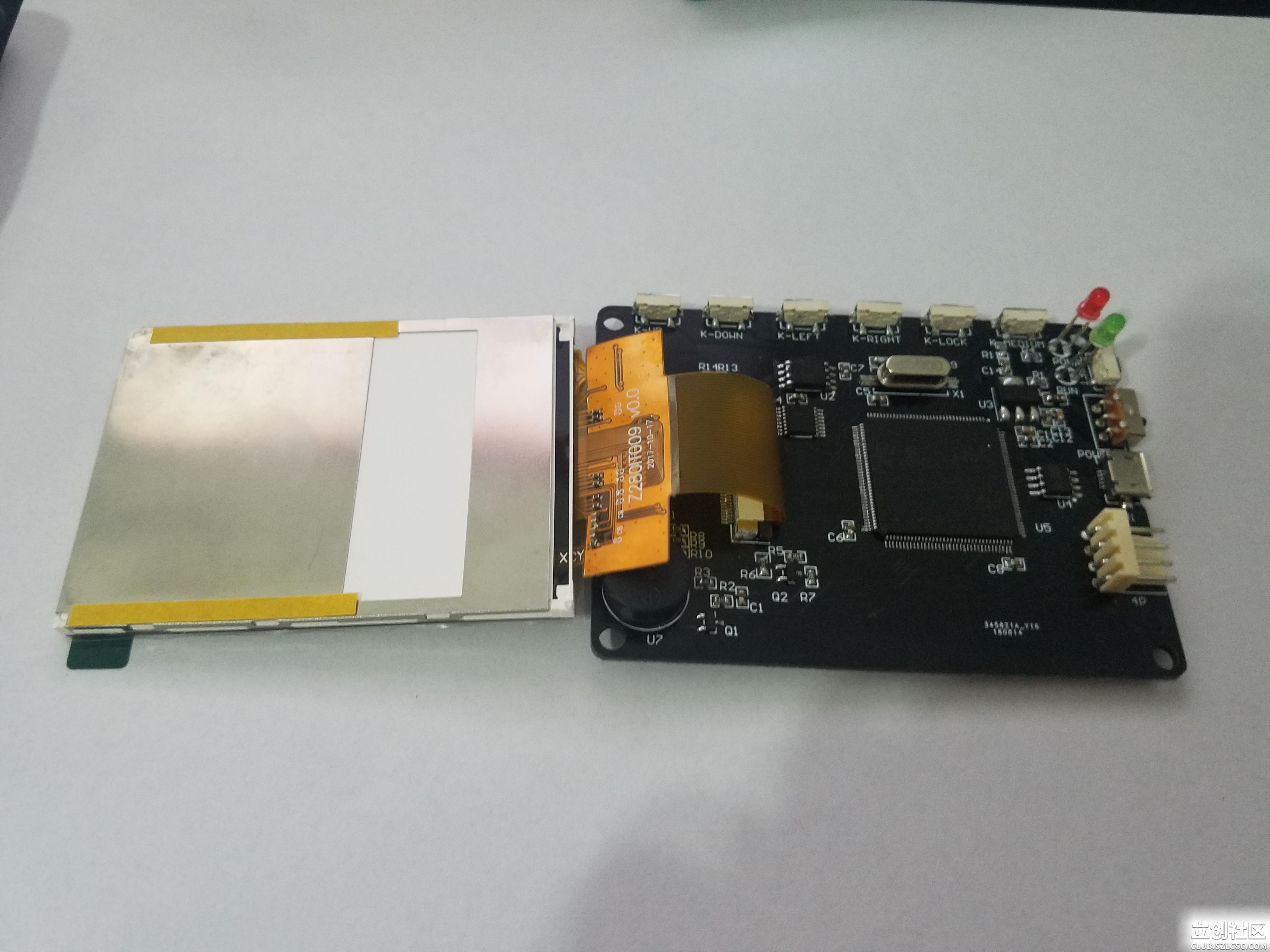
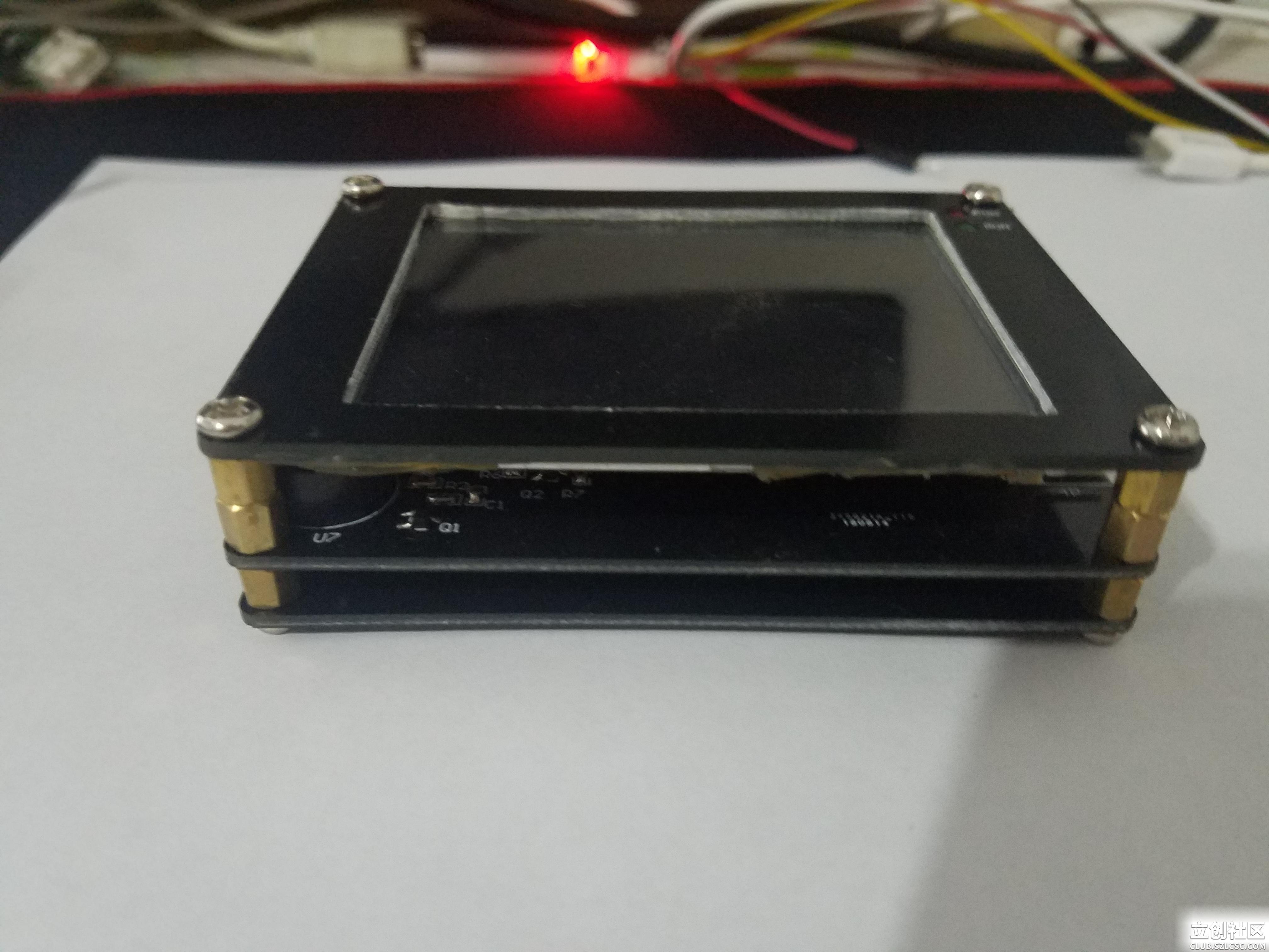
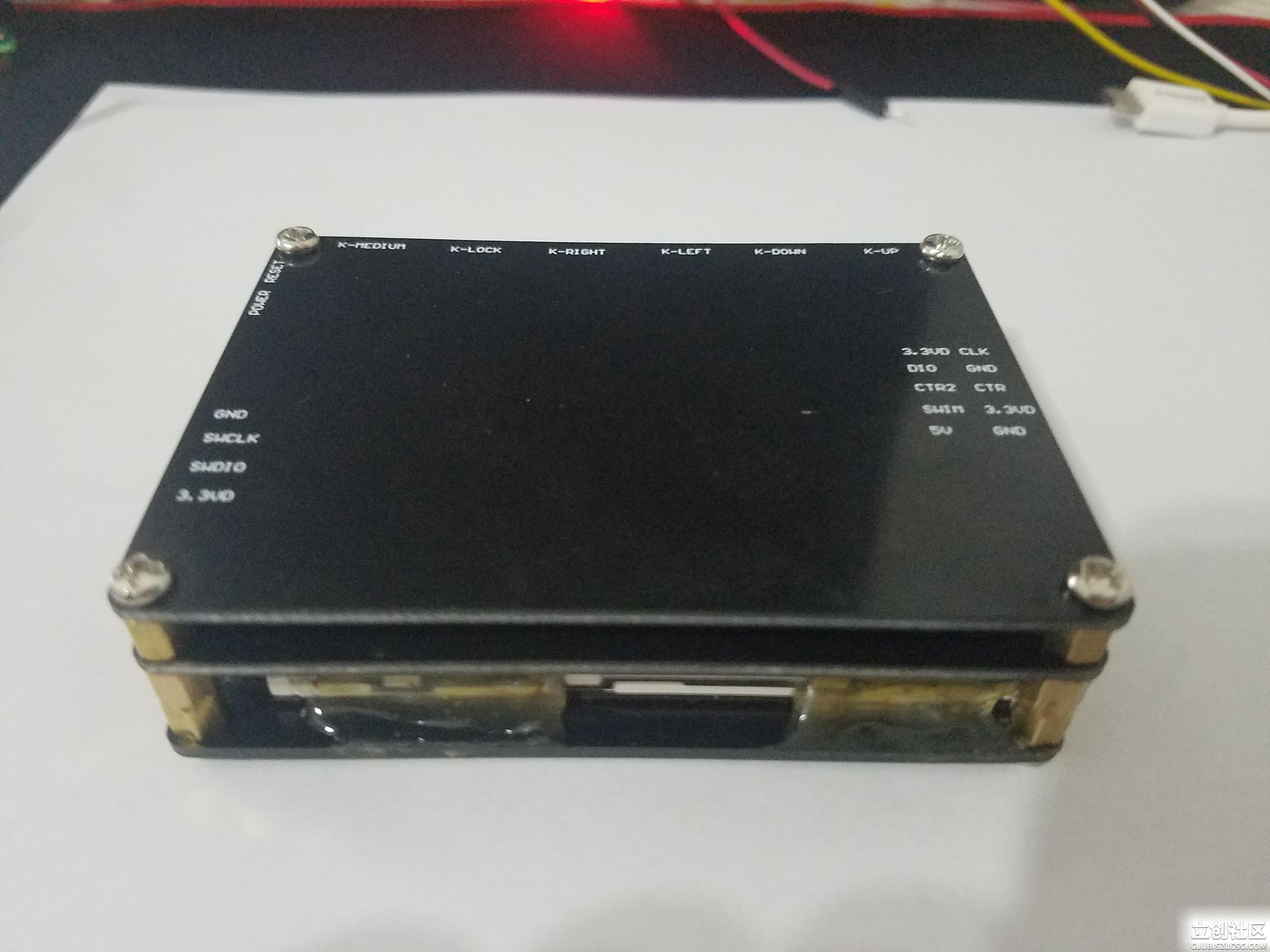
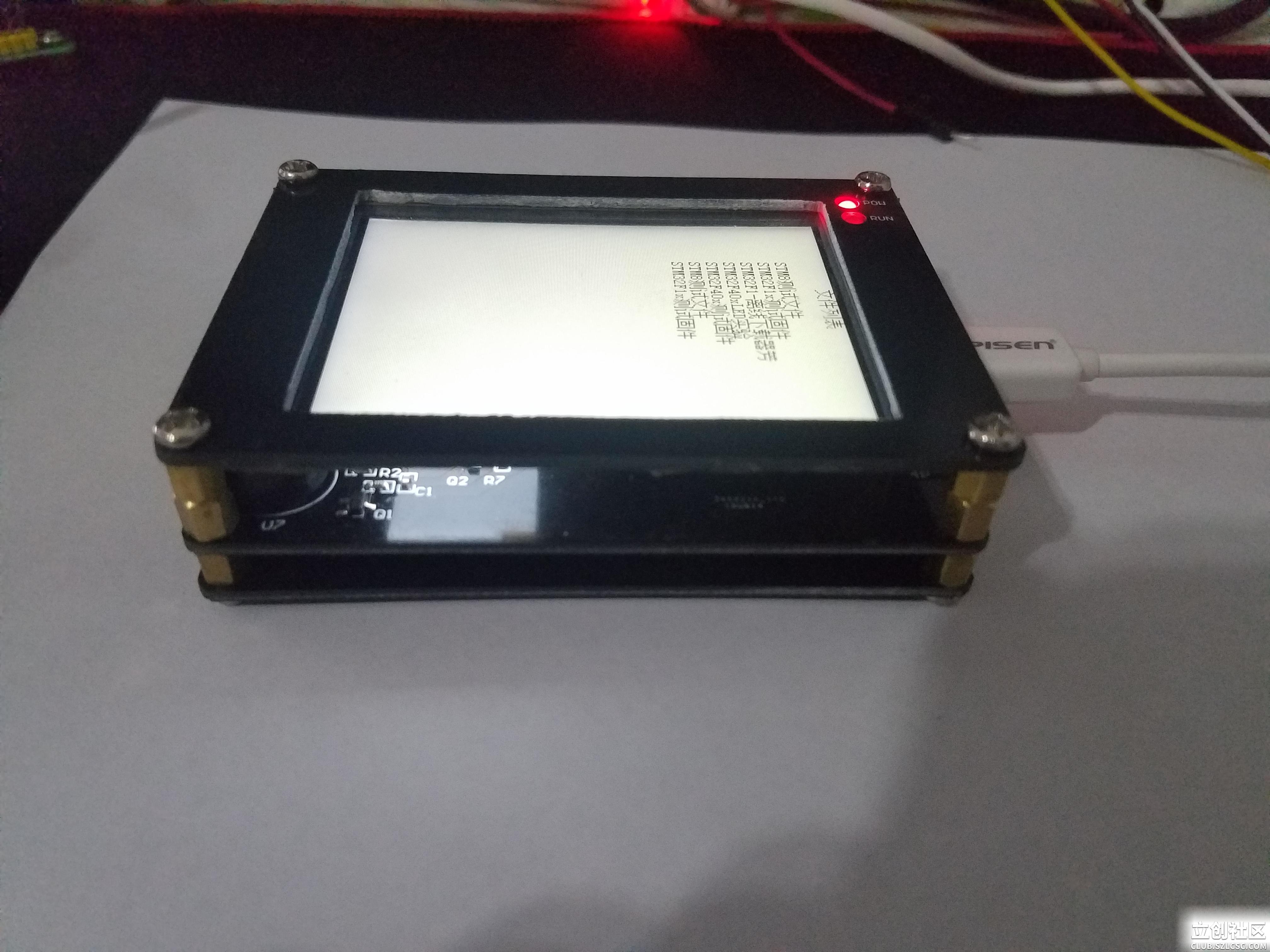
1. The appearance picture of the whole machine or the picture of the welded and assembled PCBA;
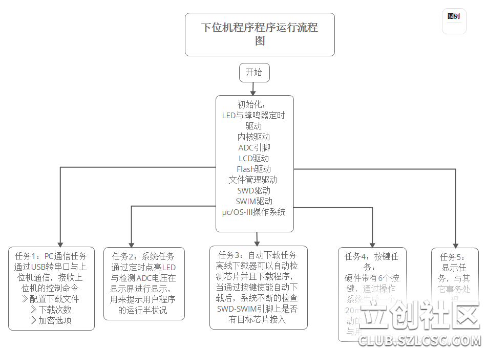
II. System architecture diagram

III. Description of the hardware part
1. Schematic diagram:
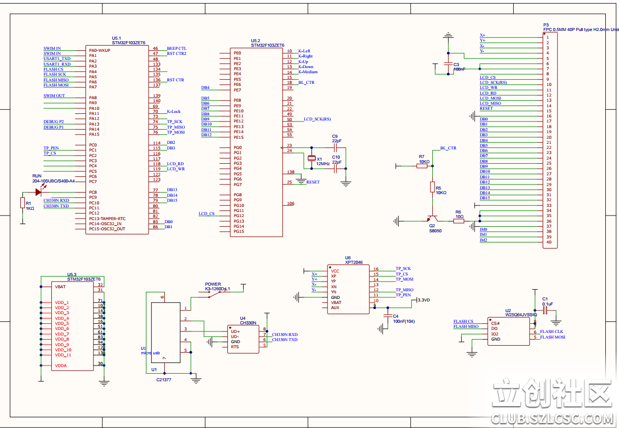
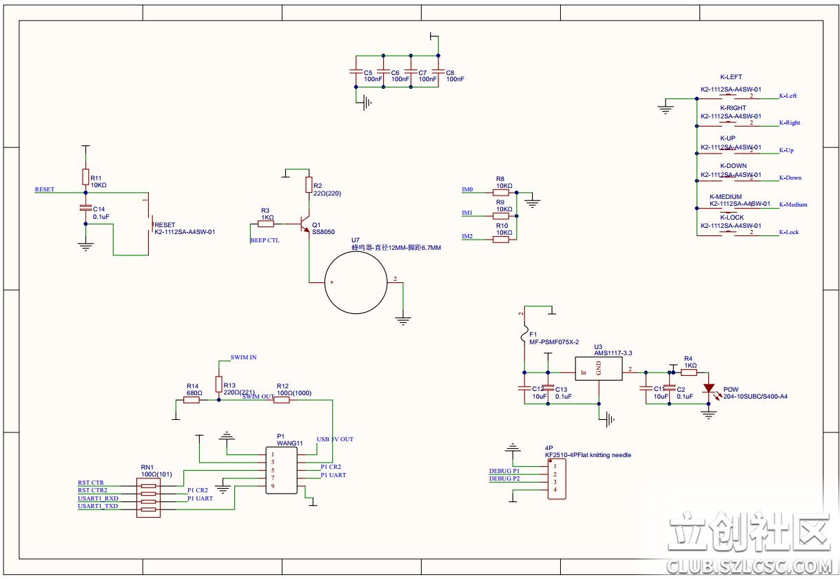
2. Implementation principle and system working process:
This offline downloader is mainly based on the SWD (Serial Wire Debug) serial debugging interface, which is used to connect the ARM core chip, and is also based on the SWIM (single wire interface module) single-line debugging module.
1): SWD interface. The STM32 series based on the Cortex-M core is widely used. Among them, the SWD debug interface is integrated. The debug interface can be used to access the bus registers and chip core inside the chip. Of course, this method can also be used to update the Flash program. The main application framework of SWD is as follows: the SWD interface is used to access the DP port, and then access its AP port through the DP port, and then access the system bus through the AP port, so as to achieve the purpose of program download.
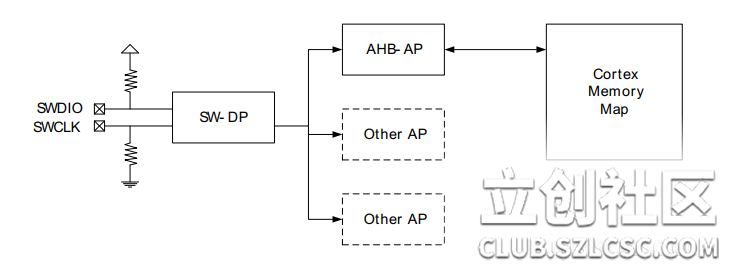

Figure 1 - SWD interface
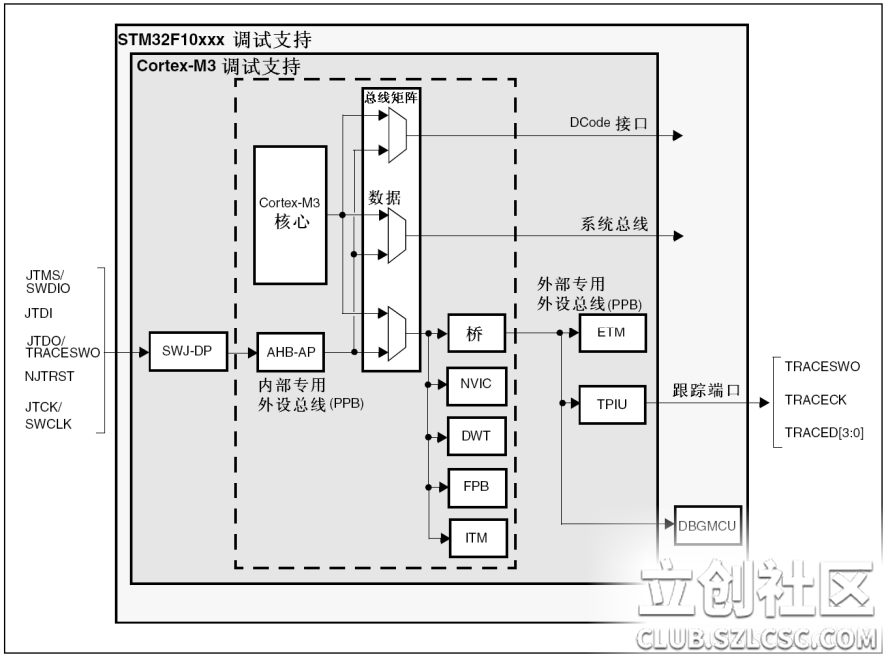
Figure 2: STM32 debug unit
SWD specific operation request: The start of the SWD command is started by 8 bits, the meaning is shown in Figure 3, start bit + AP/DP selection bit + read/write bit + two address bits + parity bit + stop bit + fixed to 1 check bit
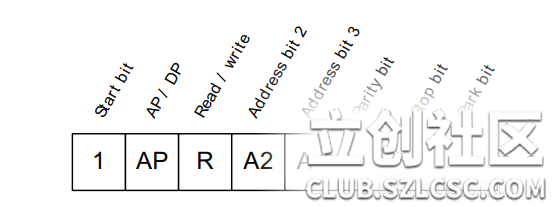

Figure 3: SWD start command

Figure 4: Read and write sequence

Figure 5, read and write sequence
2): SWIM interface. SWIM is a debug interface dedicated to the STM8 series. Only one line can be used to complete debugging and simulation. This is also because the STM8 is mainly positioned as a small microcontroller and has a high cost performance. The main block diagram of its SWIM interface is as follows:
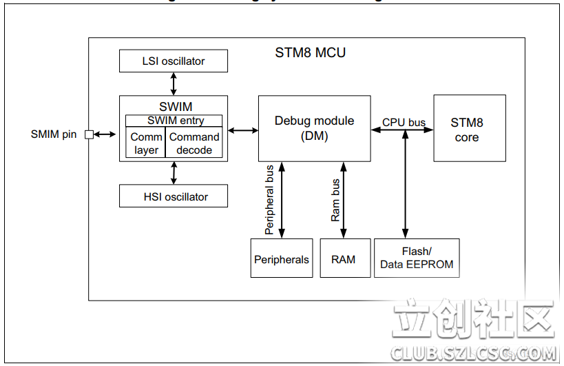
Figure 6: SWIM debug interface block diagram
Since SWIM is a single-line mode, it has very high time requirements. Its timing diagram is as follows: For this reason, a timer is deliberately used in the code to meet such operations.
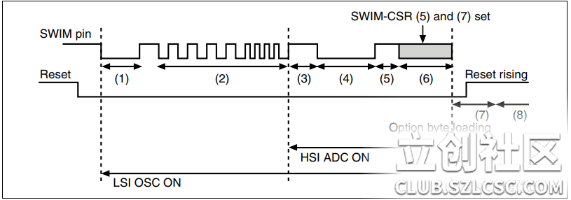
Figure 7: SWIM timing diagram
3. Indicate the name of the EDA tool software used and attach the design link.
The EDA tool used this time is: LiChuang EDA, and the open source link is as follows: https://oshwhub.com/lengyu1226/wang1111
4. Bill of Materials (BOM List)
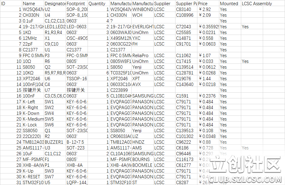

5. Description of the Software

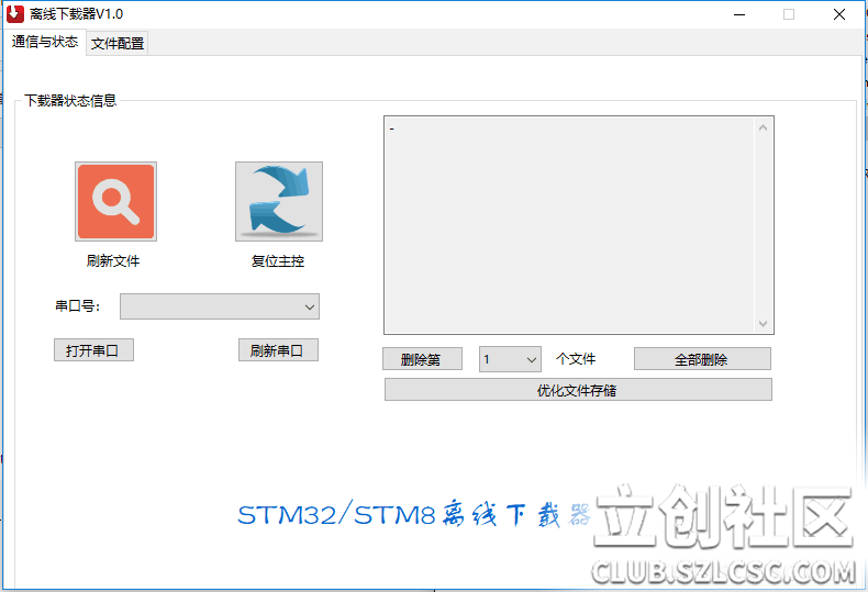
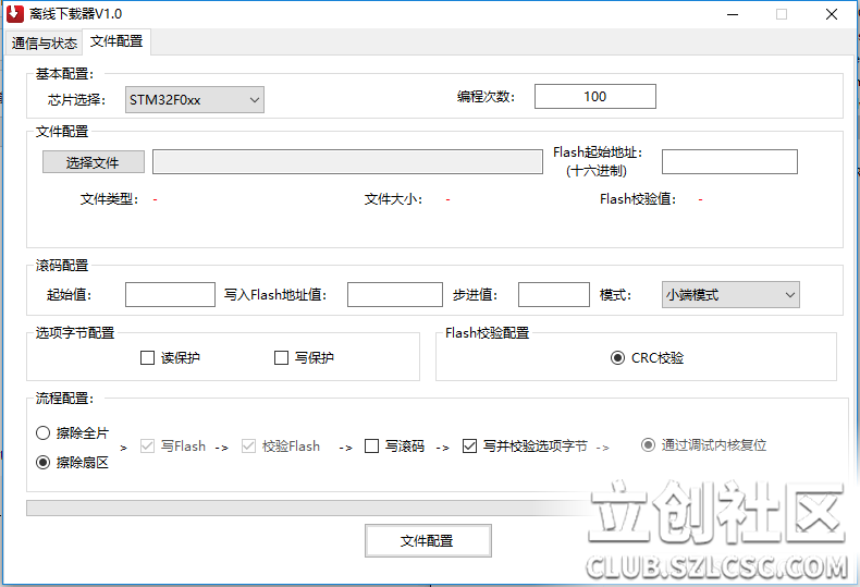
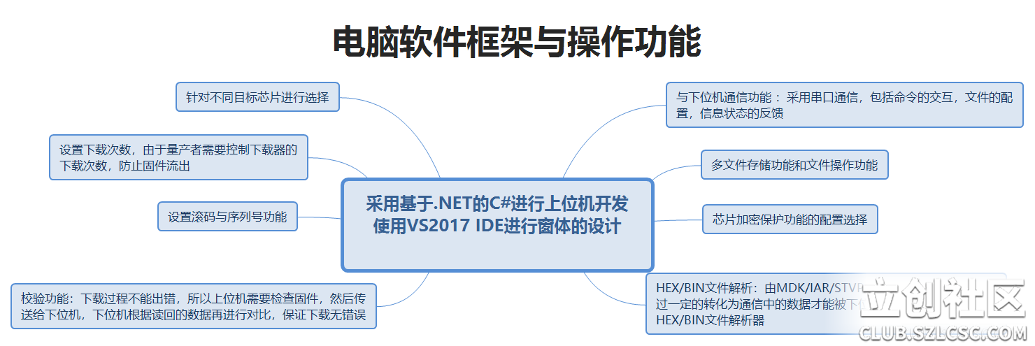
Screenshot of the host computer software:


1): Due to the huge amount of code, some core codes are posted. The following is the core code for SWD control
/**
* @B can be understood as TurnAround
*
*/
void SWDIO_CYCLE( void )
{
if( slowModeEnable == ENABLE)
{
SWD_Delay();
SWD_SWDIO_PIN_OUT = 0
; SWD_Delay();
SWD_SWDIO_PIN_OUT = 1;
SWD_Delay();
}
else
{
SWD_SWDIO_PIN_OUT = 0;
SWD_SWDIO_PIN_OUT = 1;
}
}
/**
* @B Read data from the AP or DP register
* reg: Obviously there are only 4 (tentative value range 0-3). Why does data use a pointer? Because in this way, the passed value, that is, the value pointed to by the pointer, can be changed
. * After the end: SWCLK remains at 1
*/
u32 readReg( u8 APnDPReg,u8 reg, u32 *data )
{
u8 i = 0;
u8 cb = 0; //
u8 parity; // Check value
u8 b = 0; // Bit used to read ACK
u8 ack = 0; // ACK value
u8 ret = SWD_ERROR_OK;
*data = 0;
int _APnDPReg = (int) APnDPReg;
int _read = (int) 1; // Read request value is 1
u8 A2 = reg & 0x01;
u8 A3 = ( reg>>1 ) & 0x01;
parity = ( _APnDPReg + _read + A2 + A3 ) & 0x01;
SWD_SWDIO_MODE_OUT; // Set to output mode
// SWD_SWDIO_DIR_CTR2 = BUFFER_IC_DIR_OUT; // Buffer set to output mode
{ // Start the send sequence
// Problem with the send sequence: After sending, it can be seen that SWCLK remains at 1:
WRITE_BIT( 1 );
WRITE_BIT( _APnDPReg );
WRITE_BIT( _read );
WRITE_BIT( A2 );
WRITE_BIT( A3 );
WRITE_BIT( parity );
WRITE_BIT( 0 );
WRITE_BIT( 1 ); // SWDIO = 1, SWCLK = 0, SWCLK = 1
}
{ // TurnAround
{
SWD_SWDIO_MODE_IN; // Set to input mode //
SWD_SWDIO_DIR_CTR2 = BUFFER_IC_DIR_IN; // Buffer is set to input mode
}
SWCLK_CYCLE();
}
{ // Read ACK
for( i=0;i> 8) & 0xFF, 8, 0))
{
return 3;
}
if (SWIM_HW_Out((addr_tmp >> 0) & 0xFF, 8, 0))
{
return 2;
}
for (i = 0; i < cur_len; i++)
{
if (SWIM_HW_In(&data[processed_len + i], 8))
{
return 1;
}
}
cur_addr += cur_len;
processed_len += cur_len;
}
return 0;
}
6. Demonstration of the work
A total of two videos were recorded. The first video demonstrates the operation process of the offline downloader in detail and the explanation time is longer. The second one is a relatively simple demonstration of the entire operation process.
1): http://url.cn/5ZQU77A?sf=uri
2): http://url.cn/5OXUQgP?sf=uri
VII. Summary
During the development process, three PCBs were designed using EasyEDA. The first one was not good enough in appearance, and the second one was found to be unreasonable during the test. After three changes, it was finally formed.
It is necessary to support more chip types. The current downloader can support STM32 and STM8 series, but in order to promote it in the future, it is necessary to support more chips. With such a downloader in hand, you can download multiple types of chips without multiple sets of equipment.
The SWD/SWIM debugging stage is difficult to understand, especially for the protocol part, but how to read it carefully and deeply understand the meaning, and finally find it is relatively simple, so when you encounter development problems, you must face them head-on.
8: Related information download:
1: Serial communication protocol.zip (Downloads: 325)
2: ARM Debug Interface v5 Architecture Specification.zip (Downloads: 409)
3: CD00226555.zip (Downloads: 271)
4: en.CD00173911.pdf.zip (Downloads: 255)
5: en.CD00191343.pdf.zip (Downloads: 251)
For more project details, see the link: http://club.szlcsc.com/article/details_12812_1.html
This project belongs to the Lichuang community "SuperCRJ"


 2. Implementation principle and system working process:
 Figure 1 - SWD interface
  Figure 2: STM32 debug unit
 Figure 3: SWD start command
  Figure 4: Read and write sequence
  Figure 5, read and write sequence
  Figure 6: SWIM debug interface block diagram
  Figure 7: SWIM timing diagram
 5. Description of the Software
 Screenshot of the host computer software: