The data compression system is the front-end module of the satellite data transmission subsystem, which receives and compresses the image data of the satellite-borne CCD camera. The compressed code stream is transmitted to the satellite transmitter through the fixed storage device for transmission and enters the data transmission channel. A satellite carries multiple linear array CCD cameras, the camera clock frequency is 50MHz, the frame period is 0.77ms, each frame data is 4096 bytes, and the total code rate is 725Mbps. It is required to compress the camera's image data in three compression modes: 1:1, 4:1 and 8:1. The output rate is less than 100Mbps in 8:1 mode and less than 200Mbps in 4:1 mode. In addition, the mechanical properties, thermal properties, electrical properties, etc. meet the requirements of the interface data sheet.
自2000年以来,笔者在国外著名学者Malvr提出的双正交重叠变换[1](LBT)的基础上系统地研究了整数(重叠+DCT)的块变换算法以及低复杂度的存储编码算法,使其图像压缩质量与JPEG 2000推荐的小波方法近似。由于克服了边缘效应,因而质量明显高于JPEG压缩方法,而且计算复杂度与存储量又比小波方法有显著改善。
Most of the current hardware solutions for satellite remote sensing image compression systems are based on high-performance programmable logic devices (FPGAs) [2-4]. However, the cost of the entire system is high, and FPGAs have single-particle upset effects. Therefore, the author proposes a multi- DSP + FPGA hardware design structure, using DSPs instead of FPGAs to complete the core algorithm, and only using one FPGA for management and control. The hardware design cost is relatively low.
1 Low-complexity image compression method based on biorthogonal lapped transform
1.1 Fast Integer Implementation of Biorthogonal Lapped Transform
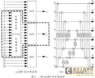
In lossy compression, the image matrix is usually first subjected to an orthogonal/biorthogonal transform to concentrate the energy distribution and make the representation more sparse. Discrete cosine transform (DCT) is widely used because of its good decorrelation effect and the existence of corresponding fast algorithms. Biorthogonal lapped transform inherits the characteristics of DCT, which is simple to calculate and has low storage requirements, while overcoming the blocking effect of DCT. Here, a fast integer implementation algorithm of biorthogonal lapped transform is proposed based on LBT [5]. All coefficients are approximated by fractions with denominators as powers of 2 and numerators as integers, so that the entire transformation process only requires integer addition and shift operations. Figure 1 shows the implementation process of one-dimensional binLBT. The two-dimensional transformation is performed in the order of rows first and columns.

1.2 Simplification and Improvement of Zerotree Coding
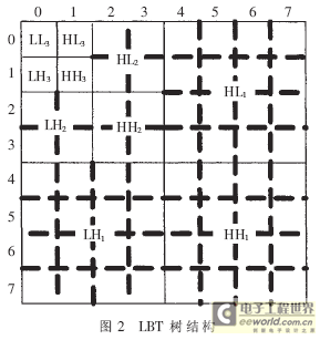
As an efficient zero-tree coding method, SPIHT divides the bit plane into sets, concentrates a large number of non-important bits 0 into several sets with specific patterns, and divides such sets containing important bits until the sets are divided into specific elements. There is a similar zero-tree structure in the LBT coefficient block. Figure 2 shows the zero-tree partitioning method in the LBT block transform that imitates the tree structure in the wavelet transform, where each wireframe corresponds to a coefficient, and the solid line divides the 64 coefficients into 10 sub-bands. Since the block transform has the effect of concentrating energy, the energy of the coefficient gradually decreases from the upper left to the lower right.

In each subband, the Golomb method is first used for encoding, and then the output code stream is input into the MQ encoder for the next step of encoding. The zerotree encoding process applies the correlation between the parent and child nodes in the zerotree structure, and it is necessary to locate its child nodes when the parent node is known. Therefore, after the LBT coefficients are output and before entering the encoder, the linear index method is used to reorder the LBT coefficients and place them in a one-dimensional array.
2 Parallel Multi-DSP+FPGA Hardware Design Solution
2.1 System hardware overall block diagram
The overall hardware block diagram of the data compression system is shown in Figure 3. 2x-1 serial CCD data enters the FPGA in parallel through the LVDS interface for timing conversion. Each DSP reads two-channel camera data from the FPGA in EDMA mode through two serial ports and caches and compresses the data. The entire data compression system requires x DSPs to process in parallel. The compressed bitstream data is output to the FPGA through the serial port. The FPGA re-caches, frames, and converts the timing before outputting it to the storage device. The interfaces for bitstream data output, remote control command input, telemetry signal output, and power supply are all connected through the backplane bus and the data transmission integrated processor .

2.2 Device Selection
The DSP selected is TMS320C6416, which is a high-performance DSP chip with a new C64XX series core launched by TI in 2000. TMS320C6416 adopts a high-performance advanced VLIW (very long instruction word) structure with 8 parallel processing units inside. Since the single instruction word length is 32 bits, 8 instructions can form an instruction package of up to 256 bits, which is distributed to 8 processing units by the internal dedicated instruction distribution module and runs simultaneously. Therefore, at a main frequency of 600MHz, the maximum processing capacity of TMS320C6416 is as high as 4800MIPS (million instructions per second)[3]. The core voltage of TMS320C6416 is 1.2V, the peripheral voltage is 3.3V, the main frequency is 400MHz~1GHz, and at a main frequency of 600MHz, it can provide 833B-level devices[6].
The FPGA uses X2V3000-5FG676C, which belongs to the VirtexTM-II series of Xlinix, with 3 million gates and 676 pins, including 484 I/O pins. The basic features of Xlinix FPGA are composed of configurable logic blocks (CLBs), input/output blocks (IOBs) and programmable interconnection resources, as well as tri-state buffers, global clock buffers and boundary scan logic. CLBs contain lookup tables (LUTs), registers and carry logic, and IOBs contain DDR registers. Memory resources mainly include distributed SelectRAM/ROM and 18KB block SelectRAM.
2.3 Interface Design
The image grayscale data of the linear array CCD camera is output in serial mode and LVDS signal level. In order to facilitate the reception of the DSP serial port, the FPGA performs level conversion and performs timing conversion according to the relevant serial protocol. The compressed image code is output through the DSP serial port, and the FPGA performs level conversion and performs corresponding conversion according to the compressor output interface timing.
The remote control machine output lines include command lines and ground lines, which are pulled up at the use end. If a negative pulse is required after the command shaping output, an additional inverter can be added or implemented inside the FPGA. The telemetry interface is divided into three parts: analog telemetry, digital telemetry, and data telemetry. Analog telemetry mainly measures the power supply (5V, 1.5V, 1.4V, etc.), and the telemetry output level is 0~5V; digital telemetry mainly measures the working status of key components in the extension, and the telemetry output level is TTL level; data telemetry mainly measures the internal operating status.
3 Key technologies and parallel processing of compression algorithms in DSP implementation
3.1 C6000 Series CPU Architecture and Pipeline
The C6000 series CPU adopts Harvard architecture, and instruction fetch and execution can run in parallel. The program bus width is 256 bits, and each instruction fetch operation fetches 8 instructions, which becomes an instruction fetch package. Instruction fetch, instruction allocation and instruction decoding are all capable of reading and transmitting 8 32-bit instructions per cycle. The C64xx series CPU has two data paths A and B, each path has 4 functional units (.L, .S, .M and .D), and instructions in different 8 functional units can be executed in parallel.
Modern microprocessors divide instructions into several sub-operations, each of which can be completed by different components inside the microprocessor. At the same time, multiple instructions can be processed in different components in an overlapping manner. This working mode is called "pipeline" working mode. The special structure of TMS320C6000 allows multiple instruction packets (up to 8 instructions per packet) to be processed in different components in an overlapping manner, greatly improving the throughput of the microprocessor.
3.2 Data type conversion and data overflow issues
TMS320C6000系列DSP的数据打包处理技术,可以使用宽长度的存储器对短字长的数据访问,这样可使编译出的代码性能显著提高。压缩算法在DSP实现中,采用short代替int来存储图像像素值和变换后的系数,并确保不会产生数据溢出。

Sum each row of |T|, the maximum is 2.8284. Perform two transformations, row and column, and the final transformation coefficient is at most 8 times the image pixel value. When the image pixel occupies 8 or 10 bits, including the sign bit, 16 bits are used to store the transformation coefficient without overflow.
3.3 Parallel Computing
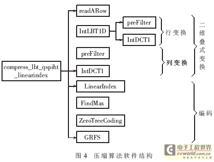
The core software structure of the compression algorithm is shown in Figure 4.

Each sub-function is written in assembly language. The key to optimizing code in C6000 series DSP is how to achieve code parallelism. In view of the instruction characteristics of C64XX series processors, the following parallel processing measures are taken:
(1) Dual channels. The processing coefficients are evenly distributed in channels A and B respectively;
(2) Data packing technology. Use LDW and STW to read and store two 16-bit coefficients at a time;
(3) Half-word operation instructions. Each instruction processes two 16-bit coefficients;
(4) Multifunctional units. The calculation of the eight coefficients in each of the two paths fully utilizes the four functional units L, S, M and D.
4 Experimental results and conclusions
A set of 40 1024×1024×8 images provided by the Chinese Academy of Sciences Remote Sensing was used as samples, and the remote sensing image compression system prototype was tested using two compression ratios of 4:1 and 8:1. The test results are as follows:
(1) When the compression ratio is 4:1, the average PSNR is above 40dB and the minimum is 38dB; when the compression ratio is 8:1, the average PSNR is above 35dB and the minimum is 32dB.
(2) For a 1024×1024×8 image, when the compression ratio is 4:1, the processing time of a single DSP is less than 64ms; when the compression ratio is 8:1, the processing time of a single DSP is less than 48ms, which is 1/30 of the time before optimization.
(3) The internal RAM of a single DSP can meet the requirements of caching 2-channel camera data and intermediate coefficients;
(4) The power consumption of a single channel is less than 0.5W, and the power consumption of the whole machine is less than 15W.
The results show that the data compression system is reasonably designed and can meet the requirements of image quality and high-speed real-time processing in actual work. However, from the results of manual image judgment, the algorithm does not retain small objects as well as JPEG2000 when compressed at 8:1. The system has now entered the prototype stage, and we hope to continue to study and optimize the algorithm, especially the encoding algorithm, to further improve the image quality.
References
[1] MALVAR H S.Biorthogonal and nonuniform lapped transforms for transform coding with reduce blocking and ringing artifacts.IEEE Transactions on Signal Processing.1998,46(4):1043-1053.
[2] Xiao Jiang. Research on satellite interferometric spectral image coding technology. Doctoral dissertation of Xidian University, 2004
[3] Chen Chao. Design and implementation of high-speed transmission image compression system. Telemetry and Remote Control, 2004, (7).
[4] Zhou Mei, Zhang Zhimin, Deng Yunkai. FPGA implementation of raw data compression module for spaceborne SAR, Modern Radar, 2006, 28(2).
[5] Zhong Guangjun, Cheng Lizhi, Chen Huowang. Integer implementation algorithm of biorthogonal lapped transform and image compression. Journal of Electronics, 2001, 29(11): 2001.
[6] TMS320C6414,TMS320C6415,TMS320C6416 FIXED-POINT DIGITAL SIGANAL PROCESSORS.Texas Instruments Incor porated,October 2002.
Previous article:C2 uses 1 CPU + 3 DSP architecture to realize network multimedia platform
Next article:Design of USB interface based on DSP platform
- Popular Resources
- Popular amplifiers
- Analysis of the application of several common contact parts in high-voltage connectors of new energy vehicles
- Wiring harness durability test and contact voltage drop test method
- Sn-doped CuO nanostructure-based ethanol gas sensor for real-time drunk driving detection in vehicles
- Design considerations for automotive battery wiring harness
- Do you know all the various motors commonly used in automotive electronics?
- What are the functions of the Internet of Vehicles? What are the uses and benefits of the Internet of Vehicles?
- Power Inverter - A critical safety system for electric vehicles
- Analysis of the information security mechanism of AUTOSAR, the automotive embedded software framework
- Brief Analysis of Automotive Ethernet Test Content and Test Methods
 Professor at Beihang University, dedicated to promoting microcontrollers and embedded systems for over 20 years.
- LED chemical incompatibility test to see which chemicals LEDs can be used with
- Application of ARM9 hardware coprocessor on WinCE embedded motherboard
- What are the key points for selecting rotor flowmeter?
- LM317 high power charger circuit
- A brief analysis of Embest's application and development of embedded medical devices
- Single-phase RC protection circuit
- stm32 PVD programmable voltage monitor
- Introduction and measurement of edge trigger and level trigger of 51 single chip microcomputer
- Improved design of Linux system software shell protection technology
- What to do if the ABB robot protection device stops
- Analysis of the application of several common contact parts in high-voltage connectors of new energy vehicles
- Wiring harness durability test and contact voltage drop test method
- From probes to power supplies, Tektronix is leading the way in comprehensive innovation in power electronics testing
- From probes to power supplies, Tektronix is leading the way in comprehensive innovation in power electronics testing
- Sn-doped CuO nanostructure-based ethanol gas sensor for real-time drunk driving detection in vehicles
- Design considerations for automotive battery wiring harness
- Do you know all the various motors commonly used in automotive electronics?
- What are the functions of the Internet of Vehicles? What are the uses and benefits of the Internet of Vehicles?
- Power Inverter - A critical safety system for electric vehicles
- Analysis of the information security mechanism of AUTOSAR, the automotive embedded software framework
- AD9144-FMC-EBZ ADI data transfer board four-channel digital-to-analog converter evaluation board module conversion
- A40i Platform Application Notes - Huawei - ME909S-4G Module Porting Application
- The news about the Agilex M series has been released for some time, but I haven’t seen any information about the specific pin packaging, etc.?
- PIC16F1824
- EEWORLD University ---- Webinar - How to quickly design power rails for Xilinx FPGA and SoC
- EEWORLD University----simulink video tutorial
- Interleaved CCM Totem Pole Bridgeless Power Factor Correction (PFC) Reference Design
- [2022 Digi-Key Innovation Design Competition] Distributed Temperature and Humidity Acquisition System-STM32H745I-DISCO Basic Learning
- Start at 2pm: TI MSP430 development training, online hands-on demo + analysis by frontline experts
- Chip Manufacturing: A Practical Tutorial on Semiconductor Process Technology (Sixth Edition)

 LM316D


 京公网安备 11010802033920号