In the early days of digital IC design (early 1960s), circuits were hand-made and schematics (diagrams) were hand-drawn using paper, pen and mimeograph. These schematics illustrated the logic gates and their associated operational functions to build the design and the connections between them.
At least one member of each design team specializes in implementation logic, minimization, and optimization, which ultimately results in replacing an entire group of communication gates to perform the same work faster or occupy less silicon chip area.
Functional verification – checking that the design works as planned – is usually performed by a group of engineers sitting around a table looking at a schematic and saying, “Eh, that looks good to me!” Similarly, timing verification – checking that the design meets the required input/output and internal path delays and does not violate any internal registers (such as setup and hold parameters) is performed with pencil and paper.
Finally, the entire set of diagrams that lay out the structure of the logic gates and the interconnections between them are all hand-drawn. These simple shapes, such as squares and rectangles, are used to make photo-masks, which are then used to make the actual silicon chip.
The earliest digital ICs were classified as "fully custom" in today's terms, because the size and shape of each geometric element that made up the individual components were hand-drawn. To address the time-consuming and error-prone shortcomings, schematic capture software packages emerged. Building digital designs at the abstract communication gate level is like creating a software program using assembly language.
The assembly process is a good implementation in terms of performance and memory capacity, but it is very time-consuming to capture and verify, and is not easily transferred to other computers for continued development. Similarly, the communication gate layer description is also time-consuming to capture and verify, and is not easily transferred to new fabs or processes.
Once the solution must be transferred to a programming language such as C for higher-level development, the high-level description will be translated into the machine language instructions required by the computer. The advantage is that it allows software developers to quickly grasp the program intent and then verify the function. In addition, programs written in C language can also be easily moved to other computer platforms.
Once digital logic designers began to move to a higher level of abstraction called RTL (Register Transfer Level), they could use logic synthesis technology, which became available in the late 1980s and early 1990s, to translate the RTL description into a corresponding netlist. This "front-end" synthesis technology was complemented by a "back-end" automated place-and-route engine that could take a netlist and perform physical construction of the design.
In small designs, the results of synthesis engines at the communication layer of abstraction may not be comparable to hand-drawn design. However, in addition to quickly and concisely grasping the design intent and greatly improving the productivity of designers, the ability of synthesis engines to automatically perform speed and area trade-offs shows that the overall performance of synthesis engines is still better than hand-drawn.
The evolution of simulation tools
Computer-aided design and verification tools for analog circuits were developed much earlier than digital circuits. The design of individual components such as transistors, resistors, capacitors, and inductors usually involves first creating a physical prototype of the design, then testing it, measuring the actual value, determining its performance, adjusting the component value, and adding/removing components as necessary to achieve the desired effect.
In the late 1960s and early 1970s, many universities and commercial companies began developing analog simulators. These programs allowed students and engineers to simulate the operation of analog circuits without actually building the circuits. The most famous early simulator was the Simulation Program with Integrated Circuit Emphasis (SPICE) developed by the University of California, Berkeley, which became very popular in the early 1970s.
Over the past few years, analog simulators have made great progress in the evolution of basic models and algorithms, as well as in the performance of simulation engines. Today's analog design and verification tools are basically limited to drawing and simulating transistor-level circuit diagrams.
• Describe analog functions at a high level of abstraction and then use these descriptions to generate transistor-level equivalent circuits.
• Automatically optimize analog circuits.
• Automatically place and route analog circuits.
The result is that most analog integrated circuits are still custom-made and hand-drawn. In addition to being expensive, time-consuming, and error-prone, this transistor-level design approach does not allow existing designs to be easily transferred to new foundries or process/technology nodes. Instead, the design migration must start from the construction of the circuit. This shows that the most advanced digital design has entered 45nm technology, but the most advanced analog design is still at 90nm, and even many analog designs are still stuck in the quagmire of 130nm and 250nm, which are technologies from 5 to 10 years ago.
Mixed Signal Tools Evolution
So far, progress in tools for true mixed-signal solutions has been slow. As mentioned earlier, to meet cost, size, weight and power requirements, analog and digital functions will be combined in a single "mixed-signal" device, and some EDA companies are trying to "bolt together" existing analog and digital simulation engines.
Traditionally, companies that specialize in digital design have tried to solve their problems by purchasing existing, proven analog solutions. The motivation was to expand market share by acquiring the customer base of analog companies, but the result was an inability to integrate a large number of scattered fragmented tools. Even in today's "latest" mixed-signal and fully customized design environments, digital and analog design teams still work in their own way, and they are completely unaware of what each other is doing. It is not uncommon for people in the two disciplines to see each other for the first time when the chip is completed, at which time the analog and digital blocks have already been placed and routed. However, chip completion is usually a manual process, including many tasks that occur before the chip goes into production (tapeout). Due to the lack of automation, the work and disposal of the chip completion usually cannot be fed back into the main design flow, resulting in major problems of reuse in future designs. (This article is provided by MAGMA Product Manager)

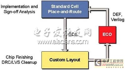
Caption: In a traditional design environment, the cycle between custom layout and standard cell placement and routing can add weeks to chip development time.

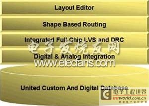
Caption: The Titan Chip Finishing system includes circuit layout editing software and provides a complete Quartz LVS verification solution.

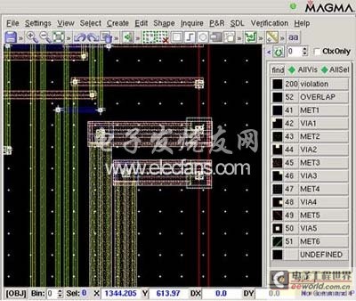
Caption: Titan automatic routing can further improve productivity.
Previous article:Application of EDA Technology in Digital System Design and Analysis
Next article:FPGA Implementation of PN Code Capture and Tracking in Direct Sequence Spread Spectrum System
Recommended ReadingLatest update time:2024-11-16 21:57


- Popular Resources
- Popular amplifiers
- Huawei's Strategic Department Director Gai Gang: The cumulative installed base of open source Euler operating system exceeds 10 million sets
- Analysis of the application of several common contact parts in high-voltage connectors of new energy vehicles
- Wiring harness durability test and contact voltage drop test method
- Sn-doped CuO nanostructure-based ethanol gas sensor for real-time drunk driving detection in vehicles
- Design considerations for automotive battery wiring harness
- Do you know all the various motors commonly used in automotive electronics?
- What are the functions of the Internet of Vehicles? What are the uses and benefits of the Internet of Vehicles?
- Power Inverter - A critical safety system for electric vehicles
- Analysis of the information security mechanism of AUTOSAR, the automotive embedded software framework
 Professor at Beihang University, dedicated to promoting microcontrollers and embedded systems for over 20 years.
- Innolux's intelligent steer-by-wire solution makes cars smarter and safer
- 8051 MCU - Parity Check
- How to efficiently balance the sensitivity of tactile sensing interfaces
- What should I do if the servo motor shakes? What causes the servo motor to shake quickly?
- 【Brushless Motor】Analysis of three-phase BLDC motor and sharing of two popular development boards
- Midea Industrial Technology's subsidiaries Clou Electronics and Hekang New Energy jointly appeared at the Munich Battery Energy Storage Exhibition and Solar Energy Exhibition
- Guoxin Sichen | Application of ferroelectric memory PB85RS2MC in power battery management, with a capacity of 2M
- Analysis of common faults of frequency converter
- In a head-on competition with Qualcomm, what kind of cockpit products has Intel come up with?
- Dalian Rongke's all-vanadium liquid flow battery energy storage equipment industrialization project has entered the sprint stage before production
- Allegro MicroSystems Introduces Advanced Magnetic and Inductive Position Sensing Solutions at Electronica 2024
- Car key in the left hand, liveness detection radar in the right hand, UWB is imperative for cars!
- After a decade of rapid development, domestic CIS has entered the market
- Aegis Dagger Battery + Thor EM-i Super Hybrid, Geely New Energy has thrown out two "king bombs"
- A brief discussion on functional safety - fault, error, and failure
- In the smart car 2.0 cycle, these core industry chains are facing major opportunities!
- The United States and Japan are developing new batteries. CATL faces challenges? How should China's new energy battery industry respond?
- Murata launches high-precision 6-axis inertial sensor for automobiles
- Ford patents pre-charge alarm to help save costs and respond to emergencies
- New real-time microcontroller system from Texas Instruments enables smarter processing in automotive and industrial applications
- 122X32LCD screen printing CBG122032AL00 driver SED1520 screen data
- [Frequently Asked Questions about iMX6ULL Development] What are the requirements for the virtual machine when setting up the iMX6ULL development environment?
- Help with domestic chips that can replace stms105C6T6
- What is the function of this op amp circuit?
- If IAR is opened slowly and has high CPU usage, it is likely that you are using the Chinese path.
- Setup and Hold Time
- I was worried for a long time after looking at the program, and it turns out that the IO port multiplexing function in ch579 does not need to be set.
- The difference between using stm32 JTAG and SWD
- Why is it easy to crack the microcontroller?
- TI-84 Plus CE Graphing Calculator to Support CircuitPython

 Introduction to Electronic Information Engineering 2nd Edition (Edited by Ye Shujiang and Liu Haicheng)
 Post-quantum cryptographic chip design (Liu Dongsheng; Zou Xuecheng; Zhang Cong, etc.)


 京公网安备 11010802033920号