The pulse wave originates from the heart beat and propagates from the heart to the peripheral arteries. The comprehensive information it presents, such as shape, intensity, rate and rhythm, largely reflects the blood characteristics of many physiological and pathological aspects of the human cardiovascular system. Heart rate is an important physiological indicator. It refers to the number of heart beats per unit time and is a physiological indicator for routine clinical diagnosis.
In order to measure the heart rate signal, there are many technologies that can be applied, such as blood measurement, heart sound measurement, ECG measurement, etc. This article discusses the use of the high opacity of blood and the great difference in light transmittance between tissue and blood, and the acquisition of pulse signals through photoelectric pulse sensors. After analog-to-digital conversion (A/D), the sampled data is digitally analyzed and processed to achieve the measurement of human heart rate.
1. Heart rate monitor system composition and working principle
The main components of the heart rate detector are shown in Figure 1. The pulse signal is collected by the photoelectric sensor, and the pulse signal data is obtained through pre-amplification, filtering, and sampling by the A/D conversion module of the microcontroller uPSD3234A and stored in the memory; the microcontroller performs digital signal processing on the obtained data and calculates the heart rate value, and the result is sent to the display module and the memory.
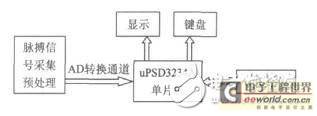
Figure 1 Schematic diagram of digital heart rate monitor
1.1 Heart rate signal acquisition preprocessing circuit
The pulse signal acquisition preprocessing circuit mainly converts the pulse wave into an electrical signal and performs preliminary high-frequency filtering preprocessing. The key part is the photoelectric pulse sensor. Photoelectric pulse sensors can be divided into two types: transmission type and reflection type according to the light receiving method.
The reflective type can not only accurately measure the changes in blood vessel volume, but also in practical applications, it only requires the sensor to touch any part of the body. When the blood flow in the irradiated area changes with the heartbeat, the infrared receiving probe will receive the arterial pulsation light pulse signal that contracts and relaxes periodically with the heart, thereby collecting the heart beat signal.
This design uses a reflective infrared sensor. As shown in Figure 2, the photoelectric pulse sensor uses infrared tubes KP-2012F3C and KP-2012P3C, which are arranged in a reflective manner. KP-2012F3C has good epidermal illumination, and the current is generally set at 20mA. The brightness is controlled by software through PWM current, which enables the infrared LED to work in the saturation area and emit light with stable light intensity.

Figure 2 Pulse signal acquisition preprocessing circuit
KP-2012P3C transistor uses AC coupling structure to enhance weak signal amplification. The signal detected by the transistor is sampled in two ways. One is the DC signal line. It is the transistor output and input to the A/D conversion channel 0 of the microcontroller through an emitter follower, which can be used to detect whether the transistor is in an effective working state; the other is the AC signal line. It is first input to the two-stage filter shaping circuit through an emitter follower and then input to the A/D conversion channel 1 of the microcontroller. The filter circuit is a two-stage bandpass filter circuit. Since the spectrum of the pulse wave contains rich pathological information, especially the spectrum in the range of 5~40Hz carries a lot of information related to coronary heart disease, considering the future expansion of functions, the upper and lower limit frequencies of the preprocessing circuit are designed to be 48Hz and 0.86Hz.
1.2 uPSD3234 MCU
This solution uses ST (STMicroelectronics)'s new single-chip microcomputer uPSD3234 as the core component of the system. It is based on the enhanced MCS-51 core 8032 single-chip microcomputer, has rich peripherals, integrates PSD (Programmable System Device, programmable peripheral device) modules, and contains large-capacity FLASH and RAM memories, integrated I2C and USB interface circuits, digital display (DDC) channels, 5 pulse width modulation (PWM) controllers, 4-channel 8-bit AD converters, programmable logic devices (PLD), and is a typical high-speed single-chip microcomputer with SOC characteristics. Therefore, it is not necessary to add complex peripheral circuits to fully meet the design requirements.
The USB module in the uPSD3234 chip supports the low-speed USB1.1 communication protocol. The heart rate monitor sampling data and the data obtained during the signal processing can be transmitted to the PC for storage and further analysis and processing.
2 Heart rate signal digital processing and algorithm
During the measurement process, the pulse signal detected by the preprocessing circuit is easily interfered by the outside world, and the interference noise needs to be processed.
Generally, there are two ways to deal with noise: one is to add a filter circuit; the other is to reduce noise through algorithms from the perspective of digital signal processing. If a filter circuit is added to the periphery, the cost will increase and affect the portability of the instrument. In addition, due to the uncertainty of interference, the filtering effect will not be very good. Although software filtering will occupy certain system resources, it has the advantages of low cost, high reliability, good stability, and flexibility, convenience, and strong functions under the condition that the processing speed allows. This article mainly uses digital filtering methods for processing, among which the most important algorithm is the matched filter algorithm.
The so-called matched filter is the best linear filter that maximizes the output signal-to-noise ratio of the filter at a specific moment and is derived from this. Matched filtering principle: Let the transfer function of the best linear filter with the largest output signal-to-noise ratio be H (ω), and the composite wave of the filter input signal and noise be:

In formula (1), s(t) is the input digital signal, whose spectrum function is S(ω), and n(t) is Gaussian noise.
Since the filter is a linear filter and satisfies the linear superposition principle, the filter output also consists of two parts: output signal and output noise, namely:

In formula (2), the spectrum function of the output signal is S0(ω), and its corresponding time domain signal is:

The average power of the filter output noise is:

Therefore, at the sampling time t0, the ratio of the instantaneous power of the linear filter output signal to the average power of the noise is:

From equation (3), it can be seen that when the input signal is given, the output signal ratio r0 is only related to the filter transfer function H (ω). According to Schwarz inequality:
According to Parseval's theorem:

In formula (5), E is the energy of the input signal, so the relationship is:

According to the condition X(ω)=kY*(ω) in Schwart's inequality, where k is an arbitrary constant, the condition X(ω)=kY*(ω) in Schwart's inequality is:

In formula (7), K is a constant, which can usually be selected as k=1.
S*(ω) is the complex conjugate of the input signal spectrum S(ω). The filter can achieve the maximum output signal-to-noise ratio of 2E/n0 at a given time t0.
The transfer function H(ω) of this filter, except for the multiplication factor Ke-jωt0, is consistent with the complex conjugate of the signal spectrum, so the filter is called a matched filter.
It is easy to get the impulse response of the matched filter:

The digital matched filtering process of the arterial pulse optical pulse signal obtained by the infrared receiving probe is realized by convolution of the input signal sequence s(n) and the impulse response sequence h(n) of the matched filter. Since the matched filter only matches the corresponding input signal, once the input signal changes, the original matched filter is no longer called a matched filter. The pulse wave is very complex, and even the pulse of the same person is not the same in every cycle, so it is necessary to design a matched filter based on the characteristics of the pulse signal. According to the formation mechanism of the pulse wave and the characteristic points of the pulse, four pulse wave differential waveforms are designed as templates for the matched filter, as shown in Figure 3. The template length is 100, which is exactly the width of the main pulse peak of the differential waveform.
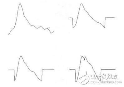
Figure 3 Matched filter template
When working, the output value of the filter to be used is determined by comparing the output results of the four templates.
This design uses the built-in ADC of uPSD3234 to sample the pre-processed pulse signal at a sampling frequency of 500Hz.
The following is a brief introduction to the entire data processing process:
1) The signal waveform obtained by sampling ADC channel 0 and channel 1 is shown in Figure 4.
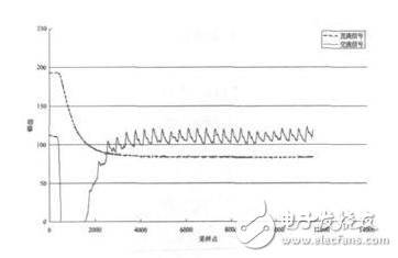
Figure 4 Waveform
2) Perform low-pass filtering on the sampled AC signal data. Since the design only realizes the function of heart rate detection, the low-pass filter cutoff frequency is designed to be 8.5Hz. Part of the waveform is shown in Figure 5.
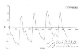
Figure 5 Low-pass filter output
3) Taking advantage of the steep rising edge of the pulse wave, it is highlighted through differential operation, and part of the waveform is shown in Figure 6.
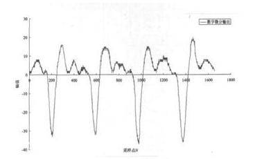
Figure 6 Digital differential waveform
4) A matched filter is required to detect the negative pulse signal in the differential waveform above. In addition, since the output value of the matched filter will vary greatly due to factors such as the user and placement of the heart rate monitor, it is also necessary to be able to automatically adjust the threshold in the design. If the signal is greater than the threshold, it is considered that a heartbeat signal is detected. The effect of the matched filter and the detection output is shown in Figure 7.
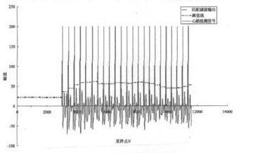
Figure 7 Matched filter output, threshold line and heartbeat detection signal
The heartbeat detection signal obtained by the above signal processing is a signal that reflects the instantaneous heartbeat of the human body. Based on this, a median algorithm can be used to accurately calculate the heart rate of the measured object. This median algorithm is: if the interval between the two pulses of the heartbeat detection signal is within the normal interval of the human heartbeat, the interval time is recorded, otherwise it is skipped. After recording enough heartbeat intervals, the median of these intervals can be calculated. The upper and lower boundaries of these intervals can be specified according to the median. The values between the upper and lower boundaries are regarded as valid interval values. When the number of valid interval values exceeds the set number, the average interval value can be calculated. Since the sampling frequency is 500Hz, each interval is 2us. A more accurate heart rate can be obtained.
3 Software Design
The system software design process is shown in Figure 8. It mainly includes display driver, key processing program, signal processing program, heart rate detection program, USB communication service program, etc.
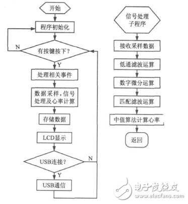
Figure 8 Software Flowchart 4 Conclusion
The reflective infrared heart rate detector designed in this scheme mainly uses the single-chip microcomputer uPSD3234 as the core component of the system, and uses digital signal processing methods such as matched filtering to obtain heart rate data, closely combining microelectronics technology with biomedical engineering technology to meet the requirements of the scheme design. In addition, this scheme has been successfully applied to fitness products treadmills, with certain innovation and practical application value, and has good market promotion value.
Previous article:Method of filtering out myoelectric interference in ECG signal detection
Next article:How to Simplify Analog Front-End Design for Heart Rate Monitors
- Popular Resources
- Popular amplifiers
- High-speed 3D bioprinter is available, using sound waves to accurately build cell structures in seconds
- [“Source” Observation Series] Application of Keithley in Particle Beam Detection Based on Perovskite System
- STMicroelectronics’ Biosensing Innovation Enables Next-Generation Wearable Personal Healthcare and Fitness Devices
- China's first national standard for organ chips is officially released, led by the Medical Devices Institute of Southeast University
- The world's first non-electric touchpad is launched: it can sense contact force, area and position even without electricity
- Artificial intelligence designs thousands of new DNA switches to precisely control gene expression
- Mouser Electronics provides electronic design engineers with advanced medical technology resources and products
- Qualcomm Wireless Care provides mobile terminal devices to empower grassroots medical workers with technology
- Magnetoelectric nanodiscs stimulate deep brain noninvasively
- Innolux's intelligent steer-by-wire solution makes cars smarter and safer
- 8051 MCU - Parity Check
- How to efficiently balance the sensitivity of tactile sensing interfaces
- What should I do if the servo motor shakes? What causes the servo motor to shake quickly?
- 【Brushless Motor】Analysis of three-phase BLDC motor and sharing of two popular development boards
- Midea Industrial Technology's subsidiaries Clou Electronics and Hekang New Energy jointly appeared at the Munich Battery Energy Storage Exhibition and Solar Energy Exhibition
- Guoxin Sichen | Application of ferroelectric memory PB85RS2MC in power battery management, with a capacity of 2M
- Analysis of common faults of frequency converter
- In a head-on competition with Qualcomm, what kind of cockpit products has Intel come up with?
- Dalian Rongke's all-vanadium liquid flow battery energy storage equipment industrialization project has entered the sprint stage before production
- Allegro MicroSystems Introduces Advanced Magnetic and Inductive Position Sensing Solutions at Electronica 2024
- Car key in the left hand, liveness detection radar in the right hand, UWB is imperative for cars!
- After a decade of rapid development, domestic CIS has entered the market
- Aegis Dagger Battery + Thor EM-i Super Hybrid, Geely New Energy has thrown out two "king bombs"
- A brief discussion on functional safety - fault, error, and failure
- In the smart car 2.0 cycle, these core industry chains are facing major opportunities!
- The United States and Japan are developing new batteries. CATL faces challenges? How should China's new energy battery industry respond?
- Murata launches high-precision 6-axis inertial sensor for automobiles
- Ford patents pre-charge alarm to help save costs and respond to emergencies
- New real-time microcontroller system from Texas Instruments enables smarter processing in automotive and industrial applications
- What do you think about RISC-V?
- DIY Energy Saving Socket Strip
- Can you recommend some 16-bit or 32-bit dual in-line microcontrollers with a price range of 2-6 yuan?
- Very pleasantly surprised, let me show you the winning nail clipper set.
- SensorTile.box accelerometer IIS3DHHCTR test project
- AD When viewing in 3D, the color cannot be changed in any way, it is just one color.
- Jiuxing shares - causes and hazards of motor bearing heating
- After the medical equipment is completed, how can we protect the security of our programs?
- How to select external clock and external memory for TI DSP?
- Can UST_OTG1 be used with a USB flash drive?

 OP413AZ/883


 京公网安备 11010802033920号