1. Bus Overview
The computer system is centered on the microprocessor. All devices must be connected to the microprocessor and must work in coordination, so the concept of bus is introduced in the microprocessor. All devices share the bus, and only one device can send data at any time (multiple devices can receive data at the same time).
The computer bus is divided into three types: control bus, address bus and data bus. The data bus is used to transmit data, the control bus is used to transmit control signals, and the address bus is used to select storage units or peripherals.
2. The three-bus structure of the microcontroller
The 51 series microcontroller has a complete bus interface timing, which can expand the control object, and its direct addressing capability reaches 64k (2 to the 16th power). In bus mode, different objects share the bus, independently address and time-share the bus. The CPU selects the object to be accessed through the address and completes the information transmission between each object.
The schematic diagram of the three-bus expansion of the microcontroller is shown in Figure 1.
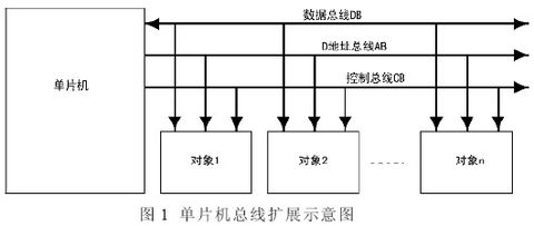
1. Data bus
The data bus of the 51 microcontroller is port P0, which is a bidirectional data channel. The CPU sends and reads data from port P0.
2. Address bus
The address bus of the 51 series microcontroller is 16 bits.
In order to save chip pins, the P0 port multiplexing method is adopted. In addition to being used as a data bus, under the timing matching of the ALE signal, the low 8-bit address is sent from the P0 port in the first half cycle of the bus access, and the 8-bit data is sent from the P0 port in the second half cycle through an external data latch.
The high 8 bits of the address are sent out through port P2.
3. Control bus
The control bus of the 51 series MCU includes the read control signal P3.7 and the write control signal P3.6, which are used as the enable signals for data reading and data writing in bus mode respectively.
3. MCU Bus Timing Analysis
51 MCU bus timing is shown in Figure 2.
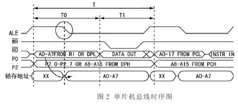
As can be seen from Figure 2, the cycle for completing a bus (read and write) operation is T. Port P0 is time-division multiplexed. During T0, port P0 sends out the lower 8-bit address, completes data latching at the falling edge of ALE, and sends out the lower 8-bit address signal. During T1, port P0 is used as a data bus to send out or read in data. The data read and write operations are completed during the low level period of the read and write control signals.
It should be noted that while the control signal (read and write signal) is valid, port P2 sends out the high 8-bit address, which cooperates with the low 8-bit address output by the data latch to realize a 16-bit address bus, that is, addressing within the 64kB range.
Since the CPU cannot perform read and write operations at the same time, the read and write signals cannot be valid at the same time. [page]
4. Common MCU addressing circuits
1. Simple address extension
The P2 port of the 51 single-chip microcomputer can be used directly as the high 8-bit address bus. In some simple system circuits, the P2 port is often used for direct addressing and driving.
The following uses the data buffer 74LS273 to drive the digital display as an example to analyze the design of the static digital display circuit driven by P2 port addressing.
The circuit of a single-digit LED digital display unit is shown in Figure 3.
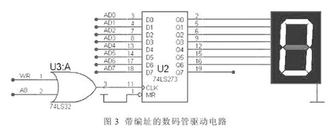
WR and A8 (P2.0) are ORed to provide the clock signal of 74LS273. When the "MOVX @DPTR, A" instruction is executed, the address information is determined by the DPTR register, and a valid write signal WR will appear. Only when the address A8 satisfies "0", the write signal can be used as the clock signal input of 74LS273 to complete data latching.
Port P2 is the 8-bit address line of A8~A15, which can be easily expanded to 8 LED digital tubes. The WR signal is connected to A8~A15 in an OR relationship. Each bit of the address line is valid at a low level, and 8 valid addresses can be realized.
The circuit of this solution is simple, but the number of valid addresses is too small, so it is not suitable for complex system design.
2. Low 8-bit address latch
The usual design circuit uses the 8D latch 74LS373 to implement address latching. The 74HC573 has the same logical function, but the pin layout is different. Using the 74HC573 is easier to wire.
The 74LS373 truth table is shown in Figure 4.
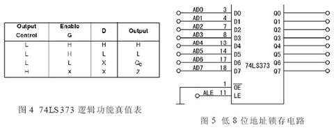
When the output enable OE is L and the control enable LE is H, the output is in the follower state;
When OE is L and LE is L, the output is in hold state.
The address latch circuit is shown in Figure 5. OE is grounded, and LE is connected to the ALE pin of the microcontroller to generate a low 8-bit address signal that meets the timing.
Executing the following three instructions will result in the timing diagram shown in Figure 6.
MOV DPTR, #0FF55H; the lower 8 bits of the address are 55H
MOV A, # 0AAH; Data to be sent 0AAH→A (55H inverted)
MOVX, @DPTR, A; 0AAH in A is sent to the object with address 0FF55H.

As can be seen from Figure 6, port P0 sends 55H first, and the address is latched at the falling edge of ALE, and then the data 0AAH is sent out. During the WR valid (low level) period, the latch outputs the lower 8-bit address 55H, and port P0 sends out the data 0AAH.
3. Complex address interface circuit with decoder
Theoretically, the high 8-bit address line can generate 256 valid addresses. How to achieve address "extension"? The accurate description of address extension is address decoding. For example, 3 address lines can be decoded into 8 addresses, and 4 lines can be decoded into 16 valid addresses. Here, a 3-8 decoder is selected to implement address decoding. The circuit diagram and corresponding addressing are shown in Table 1.

5. MCU bus addressing circuit example
Single chip microcomputer system with bus expansion interface, including external 32k RAM expansion, LCD1602 interface, input and output ports.
The minimum system circuit of the single-chip microcomputer with address expansion is shown in Figure 7. [page]

Use 74HC573 to latch the lower 8 bits of the address; 74138 implements 8 address extensions. A, B, and C of 74138 are connected to A8~A10, E1 is connected to A15, and E2 and E3 are grounded, which is always valid, and 8 addresses from 0F8FFH to 0FFFFH are obtained (don't care bits are represented by 1) or 8000H to 8700H (don't care bits are represented by 0).
The 32k RAM interface is shown in Figure 8.
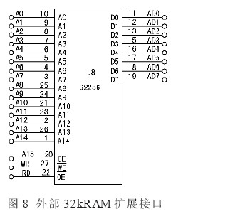
D0~D7 are connected to the data bus P0 port, address lines A0~A14 are connected to the lower 15 bits of the microcontroller address bus, and microcontroller address line A15 is connected to the RAM chip select signal, which is valid at low level. In this way, the RAM address is allocated from 0000H to 7FFFH, which does not conflict with the 74138 decoding address.
The LCD1602 interface circuit is shown in Figure 9.

RS and RW are connected to A12 and A13 respectively, and the enable signal addressing is Y7. In this way, the four drive addresses (data read and write and command read and write) of the LCD are 0CFFFH to 0FFFFH (don't care bit is 1) or 8700H to 0B700H (don't care bit is 0).
Sometimes the microcontroller pins are not enough and need to be expanded. The input port expansion circuit is shown in Figure 10.

By utilizing the high impedance function of 74HC573 (74LS373), its outputs Q0~Q7 are connected to port P0. When the bus address read operation is satisfied, the data input to InPORT can be read into the accumulator of the microcontroller, with the address being 0F8FFH or 8000H.
The output port expansion circuit is shown in Figure 11.

By using the data latch function of 74LS273, the data in the microcontroller accumulator can be written into the 273 latch output when the bus address is written. The address is 0F8FFH or 8000H. Due to the different control buses used, the address can be shared with the input.
VI. Conclusion
Bus extension is a technology that must be mastered when designing microcontroller control circuits. A large number of special function ICs support bus interfaces, such as ADC0809, TLC7528, DDS device AD9851, etc.
The key point of the bus interface is that the bus is time-division multiplexed under strict timing control to achieve complex system design.
Previous article:51 MCU external expansion RAM
Next article:Single chip dynamic scanning display circuit
- Popular Resources
- Popular amplifiers
-
 USB Complete The Developer\'s Guide 5ed (USB Development Complete 5th Edition)
 -
 Multi-channel pressure measuring instrument based on C8051F020 single chip microcomputer
 -
 Data Acquisition System Based on ISA Bus and KH-9300
 -
 Design of automatic player for work and rest signal based on 51 single chip microcomputer
 Professor at Beihang University, dedicated to promoting microcontrollers and embedded systems for over 20 years.
- Innolux's intelligent steer-by-wire solution makes cars smarter and safer
- 8051 MCU - Parity Check
- How to efficiently balance the sensitivity of tactile sensing interfaces
- What should I do if the servo motor shakes? What causes the servo motor to shake quickly?
- 【Brushless Motor】Analysis of three-phase BLDC motor and sharing of two popular development boards
- Midea Industrial Technology's subsidiaries Clou Electronics and Hekang New Energy jointly appeared at the Munich Battery Energy Storage Exhibition and Solar Energy Exhibition
- Guoxin Sichen | Application of ferroelectric memory PB85RS2MC in power battery management, with a capacity of 2M
- Analysis of common faults of frequency converter
- In a head-on competition with Qualcomm, what kind of cockpit products has Intel come up with?
- Dalian Rongke's all-vanadium liquid flow battery energy storage equipment industrialization project has entered the sprint stage before production
- Allegro MicroSystems Introduces Advanced Magnetic and Inductive Position Sensing Solutions at Electronica 2024
- Car key in the left hand, liveness detection radar in the right hand, UWB is imperative for cars!
- After a decade of rapid development, domestic CIS has entered the market
- Aegis Dagger Battery + Thor EM-i Super Hybrid, Geely New Energy has thrown out two "king bombs"
- A brief discussion on functional safety - fault, error, and failure
- In the smart car 2.0 cycle, these core industry chains are facing major opportunities!
- The United States and Japan are developing new batteries. CATL faces challenges? How should China's new energy battery industry respond?
- Murata launches high-precision 6-axis inertial sensor for automobiles
- Ford patents pre-charge alarm to help save costs and respond to emergencies
- New real-time microcontroller system from Texas Instruments enables smarter processing in automotive and industrial applications
- 100% Earn E-Coins or Red Packets: Tektronix will help you solve USB development and testing problems. Download, complain/share experiences to win good gifts
- 【NXP Rapid IoT Review】 NO5. Development Kit Hardware Module Review
- Linux self-study notes (I) Please criticize and correct me, and learn together
- How to prevent copying of FPGA code running on the board
- Application of MSP430F5xxx in the highway toll collection system (ETC)
- Today is World Environment Day
- TI TMS320F2812 SVPWM Program
- High impedance circuit protection issues
- MCU drives 24V solenoid valve
- The PWM output signal of the 28335 chip is always high

 USB Complete The Developer\'s Guide 5ed (USB Development Complete 5th Edition)
 Multi-channel pressure measuring instrument based on C8051F020 single chip microcomputer


 京公网安备 11010802033920号