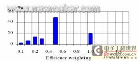
Figure 1: European efficiency calculation ratio
Selection of power devices
In the design of general inverters, IGBT is the most commonly used device, considering the cost-effectiveness factor. Because of the nonlinear characteristics of the IGBT conduction voltage drop, the IGBT conduction voltage drop does not increase significantly with the increase of current. This ensures that the inverter can still maintain low losses and high efficiency under maximum load conditions. However, for photovoltaic inverters, this characteristic of IGBT has become a disadvantage. Because the European efficiency is mainly related to the efficiency of the inverter under different light load conditions. Under light load, the on-state voltage drop of the IGBT does not drop significantly, which reduces the European efficiency of the inverter. On the contrary, the on-state voltage drop of the MOSFET is linear, and it has a lower on-state voltage drop under light load conditions. In addition, considering its excellent dynamic characteristics and high-frequency working ability, MOSFET has become the first choice for photovoltaic inverters. In addition, considering the huge economic returns after improving the European efficiency, the latest relatively expensive devices, such as SiC diodes, are also being used more and more in the design of photovoltaic inverters. SiC Schottky diodes can significantly reduce the conduction loss of the switch tube and reduce electromagnetic interference.
Design goals of photovoltaic inverters
For transformerless photovoltaic inverters, its main design goals are:
· Track the maximum power point of the solar cell input voltage to obtain the maximum input power
· Pursue the maximum European efficiency of the photovoltaic inverter
· Low electromagnetic interference
In order to obtain the maximum input power, the circuit must have the function of automatically adjusting the input voltage according to different sunlight conditions. The maximum power point is generally around 70% of the open-loop voltage. Of course, this is also related to the characteristics of the specific photovoltaic cells used. The typical circuit is realized through a boost circuit. Then the DC power is inverted into a grid-connectable sinusoidal AC power through an inverter. Introduction to the topology of
single-phase transformerless photovoltaic inverters The choice of topology is related to the rated output power of the photovoltaic inverter. For photovoltaic inverters below 4kw, a topology with a DC bus not exceeding 500V and a single-phase output is usually selected.

Figure 2: Functional diagram of a single-phase transformerless photovoltaic inverter
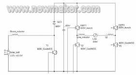
Figure 3: Schematic diagram of a single-phase transformerless photovoltaic inverter

Figure 4: flowSOL-BI – boost circuit and full-bridge inverter circuit
Boost circuit consists of MOSFET (600V/45mΩ) and SiC diode
The bypass diode is mainly used to bypass the Boost circuit when the input exceeds the rated load, thereby improving the overall efficiency of the inverter.
The upper half of the H-bridge circuit consists of 75A/600V IGBT and SiC diode, and the lower half consists of MOSFET (600V/45mΩ)
Integrated temperature detection resistor
Efficiency calculation of flowSOL0-BI, a dedicated module for single-phase transformerless photovoltaic inverter
Here we mainly consider the loss of power semiconductors, and the loss of other passive devices, such as Boost inductors and output filter inductors, is not included. Based
on the relevant parameters of this circuit, the simulation results are as follows:
Conditions:
Pin=2kW
fPWM = 16kHz
VPV-nominal = 300V
VDC = 400V
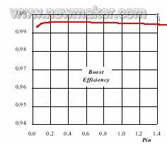
Figure 5: Boost circuit efficiency simulation result EE=99.6%
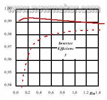
Figure 6: flowSOL-BI inverter circuit efficiency simulation results – EE=99.2%
Standard IGBT full bridge – EE=97.2% (dashed line)
Introduction to the topology of three-phase transformerless photovoltaic inverter
High-power photovoltaic inverters require the use of more photovoltaic battery groups and three-phase inverter outputs (Figure 7), and the maximum DC bus voltage will reach 1000V.

Figure 7: Functional diagram of a three-phase transformerless photovoltaic inverter
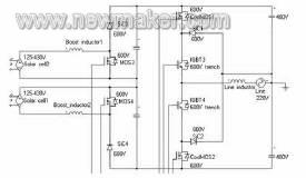
Figure 8: Schematic diagram of a three-phase transformerless NPC photovoltaic inverter
Dual-Boost module technical parameters (Figure 9):
The dual-Boost circuit is composed of MOSFET (600V/45 mΩ) and SiC diode.
The bypass diode is mainly used to bypass the Boost circuit when the input exceeds the rated load, thereby improving the overall efficiency of the inverter.
The module integrates a temperature detection resistor

The middle switching link is composed of 75A/600V IGBT and fast recovery diode. The
upper and lower high-frequency switching links are composed of MOSFET (600V/45 mΩ).
The center point clamping diode is composed of SiC diode.
The module has an integrated temperature detection resistor.
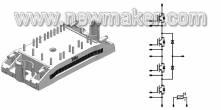
Figure 10: flowSOL-NPI – NPC inverter bridge
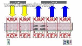
Figure 11: Layout of dual boost modules in parallel and three-phase NPC inverter output module
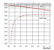
Figure 12: Comparison of NPC inverter bridge output efficiency (solid line) and half-bridge inverter efficiency (dashed line)
Introduction to the design ideas of the next generation photovoltaic inverter topology
At present, the hybrid H-bridge (MOSFET + IGBT) topology has achieved a high efficiency level. The next generation of photovoltaic inverters will focus on the following performance improvements:
further improvement of efficiency
Reactive power compensation
Efficient bidirectional conversion mode
Single-phase photovoltaic inverter topology
For single-phase photovoltaic inverters, we first discuss how to further improve the efficiency of the hybrid H-bridge topology (as shown in Figure 13).
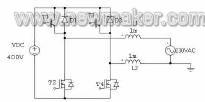
Figure 13: Development of PV inverters – hybrid
Since the IGBT of the upper bridge arm operates at a switching frequency of 50Hz, it is actually not necessary to filter this branch. Therefore, the circuit topology is optimized to obtain the emitter open circuit topology shown in Figure 14. The advantage of this topology is that only the branch with high-frequency current passing through has a filter inductor, thereby reducing the loss of the output filter circuit.

Figure 14 Improved transformerless upper bridge arm open emitter topology

Figure 15: flowSOL0-BI-open E (P896-E02)
boost circuit is composed of MOSFET (600V/45 mΩ) and SiC diode.
The bypass diode is mainly used to bypass the Boost circuit when the input exceeds the rated load, thereby improving the overall efficiency of the inverter.
The upper arm of the H bridge uses IGBT (600V/75A) and SiC diode, and the lower arm uses MOSFET (600V/45 mΩ).
The module has an internal integrated temperature detection resistor
. Let's analyze the emitter open circuit topology shown in Figure 14. When the MOSFET of the lower arm is working, the diode connected in anti-parallel with the IGBT of the upper arm does not work due to the effect of the filter inductor. In this way, MOSFET can also be used in the upper arm to improve the efficiency of the inverter when the load is light. The simulation results show that at a rated power output of 2kW, the European efficiency of this photovoltaic inverter can be increased by 0.2%, so that the efficiency reaches 99.4%. In actual applications, this topology will improve efficiency more, because the simulation results are obtained under the assumption that the chip junction temperature is 125℃, but due to the large size of MOSFET and the fact that photovoltaic inverters often work under light load, the MOSFET chip junction temperature is much lower than 125℃, so the on-resistance RDS-on of MOSFET in actual operation will be lower than the value in simulation, and the loss will be smaller accordingly. How to solve the problem of reactive power? The only way to handle reactive power with this circuit topology is to use FRED-FET, but the on-resistance RDS-on of these devices is usually very high. Another disadvantage is that its reverse recovery characteristics are poor, which affects the performance during reactive compensation and bidirectional conversion. However, in some special applications, if reactive power must be used to measure line impedance or protect certain components, the topology shown in Figure 16 will meet the above requirements.
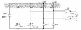
Figure 16: All-MOSFET topology for reactive loads

Figure 17: European efficiency of different topologies at 2kW rated power
Similar improvements can be made to the three-phase photovoltaic inverter of NPC topology.
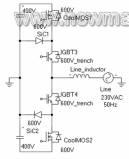
Figure 18: Three-level inverter
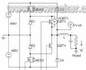
Figure 19: NPC topology inverter capable of reactive power output
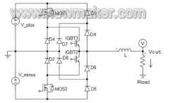
Figure 20: NPC topology inverter for reactive power output (adding 2 SiC diodes and 4 Si diodes)
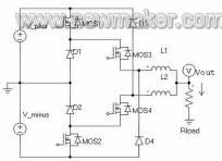
Figure 21: NPC topology inverter using MOSFET to achieve reactive power output
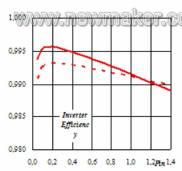
Figure 22: Efficiency comparison of all-MOSFET solution and hybrid solution at rated power of 2kW
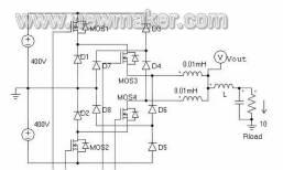
Figure 23: NPC inverter topology using 2 SiC diodes, 4 Si diodes and separate outputs
Previous article:Knowledge summary: Some tips on power factor correction
Next article:A High Precision BiCMOS Current Mode Bandgap Reference
Recommended ReadingLatest update time:2024-11-16 16:34
![Power-One communication power monitoring system communication protocol cracking [Figure]](https://6.eewimg.cn/news/statics/images/loading.gif)

- Popular Resources
- Popular amplifiers
- MathWorks and NXP Collaborate to Launch Model-Based Design Toolbox for Battery Management Systems
- STMicroelectronics' advanced galvanically isolated gate driver STGAP3S provides flexible protection for IGBTs and SiC MOSFETs
- New diaphragm-free solid-state lithium battery technology is launched: the distance between the positive and negative electrodes is less than 0.000001 meters
- [“Source” Observe the Autumn Series] Application and testing of the next generation of semiconductor gallium oxide device photodetectors
- 采用自主设计封装,绝缘电阻显著提高!ROHM开发出更高电压xEV系统的SiC肖特基势垒二极管
- Will GaN replace SiC? PI's disruptive 1700V InnoMux2 is here to demonstrate
- From Isolation to the Third and a Half Generation: Understanding Naxinwei's Gate Driver IC in One Article
- The appeal of 48 V technology: importance, benefits and key factors in system-level applications
- Important breakthrough in recycling of used lithium-ion batteries
- Innolux's intelligent steer-by-wire solution makes cars smarter and safer
- 8051 MCU - Parity Check
- How to efficiently balance the sensitivity of tactile sensing interfaces
- What should I do if the servo motor shakes? What causes the servo motor to shake quickly?
- 【Brushless Motor】Analysis of three-phase BLDC motor and sharing of two popular development boards
- Midea Industrial Technology's subsidiaries Clou Electronics and Hekang New Energy jointly appeared at the Munich Battery Energy Storage Exhibition and Solar Energy Exhibition
- Guoxin Sichen | Application of ferroelectric memory PB85RS2MC in power battery management, with a capacity of 2M
- Analysis of common faults of frequency converter
- In a head-on competition with Qualcomm, what kind of cockpit products has Intel come up with?
- Dalian Rongke's all-vanadium liquid flow battery energy storage equipment industrialization project has entered the sprint stage before production
- Allegro MicroSystems Introduces Advanced Magnetic and Inductive Position Sensing Solutions at Electronica 2024
- Car key in the left hand, liveness detection radar in the right hand, UWB is imperative for cars!
- After a decade of rapid development, domestic CIS has entered the market
- Aegis Dagger Battery + Thor EM-i Super Hybrid, Geely New Energy has thrown out two "king bombs"
- A brief discussion on functional safety - fault, error, and failure
- In the smart car 2.0 cycle, these core industry chains are facing major opportunities!
- The United States and Japan are developing new batteries. CATL faces challenges? How should China's new energy battery industry respond?
- Murata launches high-precision 6-axis inertial sensor for automobiles
- Ford patents pre-charge alarm to help save costs and respond to emergencies
- New real-time microcontroller system from Texas Instruments enables smarter processing in automotive and industrial applications
- Analysis of previous "Instrumentation" competition topics
- Hard work pays off? TMS320F28379D debugging experience
- EEWORLD University ---- [Open Source Sao Ke] FPGA-based SDRAM controller design (SDRAM Season 1)
- 【Qinheng Trial】549+ Light up a lamp first
- LED constant current driver chip recommendation
- SONY ICD-SX2000 Voice Recorder Disassembly
- Gated Clock.rar
- Battery explosion problem
- What is the difference between a thermocouple and a RTD?
- EEWORLD University Hall----Live playback: Bidirectional CLLLC resonance, dual active bridge (DAB) reference design

 Hardware Accelerators in Autonomous Driving
 Digilent Vivado library


 京公网安备 11010802033920号