In recent years, the application of light-emitting diodes ( LEDs ) has been growing, and its market coverage is very wide, including automotive lighting applications such as indicator lights, spotlights and headlights, photographic functions such as display backlights and camera flashes, consumer products such as LED display backlights and projection systems, architectural applications such as building feature lighting and signs, and many other applications. LEDs have high brightness, high luminous efficiency and fast response speed. Due to their low energy consumption, long service life, low heat release and ability to emit colored light, they have replaced incandescent lamps in many aspects.
As LED efficiency continues to improve, the amount of lumens per watt produced continues to increase, and the use of LEDs for general lighting is becoming more and more practical. For example, in 2003, a fluorescent tube equivalent to 3,000 lumens required more than 1,300 LEDs with an efficiency of 30 lumens per watt to achieve the same effect. But by 2005, the number of LEDs required to achieve the same fluorescent tube lighting effect was reduced by 20 times to only about 50, each with a luminous efficiency of 50 lumens per watt or higher and a luminous intensity of 60 lumens.
LED lighting levels
There are four stages, or areas, in LED production. The first stage is called Product Stage 0, which refers to the production of the device itself. The second stage, Product Stage 1, is the primary packaging, which refers to connecting the device to the power source through die attach and wire bonding to form a surface mount package. The third stage, Product Stage 2, refers to the secondary packaging. Multiple primary packages are put together to form the light output required for applications such as external signals or outdoor lighting. The fourth stage, Product Stage 3, is the system packaging of the entire system or solution.
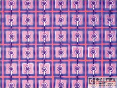
Primary LED packaging includes packaging of single LEDs and complex LED matrices. In a standard LED array, each LED is connected to a substrate electrode. The LEDs can be processed separately or connected together. Most of this type of packaging uses epoxy to adhere the chip. For high-brightness LED applications, such as outdoor lighting or tail projection screen lighting, a matrix structure of LEDs is required. In this structure, the LEDs are arranged in tight rows and columns to obtain as much light as possible. Figure 1 is a diagram of an LED matrix, which together can emit a huge amount of lumens. The number and tightness of the LEDs require good thermal conductivity of the chip attach material to keep the LED as cool as possible.

Figure 1 LED matrix diagram
Matrix LED packages are the basis of many systems in production. Their recent popularity is due to the ability to achieve more lumens per watt of power with this structure. However, compared to single-chip packages, matrix LED packages present significant challenges for die attach adhesives and wire bonding. High-brightness LED applications require maximum heat transfer to meet performance requirements.
Packaged high brightness LED
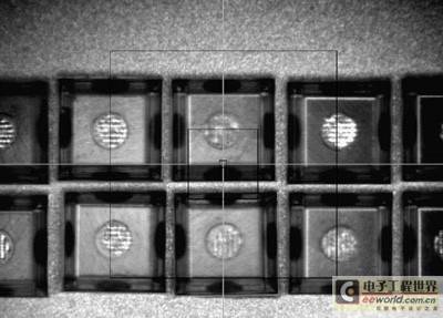
The matrix LED process steps include material preparation, chip placement, pulse reflow, cleaning, wire bonding and testing. The following discussion will focus on the pulse reflow (low temperature eutectic bonding) and wire bonding steps. The example is a 9 8 290 μm LED matrix using AuSn bonding. The LEDs are electrically connected together in the column direction. The purpose is to use metallurgical eutectic interconnects to connect the LEDs and substrates together, and arrange the LEDs as closely as possible based on component tolerances (about 1 mil gap). Figure 2 shows the 290 μm LED matrix.

Figure 2 290 micron LED attached to AuSn before wire bonding. Pulse reflow
The key to LED packaging is to avoid holes in the eutectic solder between the diode and its substrate. The thermal and electrical connections required for stable light transmission are completed by the solder. The eutectic chip adhesive transfers the huge heat energy generated by the diode to maintain the thermal stability of the device. Controlling the eutectic bonding process is the key to achieving high yield and reliability.
Precise eutectic part bonding involves diode pick and place, in-situ reflow of pre-molded or pre-tinned devices with programmable x, y or z-axis stirring, and programmable pulsed heating or steady-state temperature. To achieve an optimized heat conduction solder interface, the temperature profile of the bonding process must be repeatable and capable of high temperature ramp rates. When the interface temperature rises to the appropriate eutectic temperature, the heating mechanism must maintain the set temperature with minimal temperature overshoot. After a required reflow time, the heating mechanism must be able to control cooling to minimize damage to the diode and allow the eutectic material to reach metallurgical equilibrium. This balance is achieved by the simultaneous application of active thermoelectric pulse heating and cooling gases.
LED matrix packaging is a very temperature sensitive process that requires careful control during the packaging process. The reflow temperature profile of the on-site eutectic die bonding process is designed to provide a constant melt and void-free bonding interface. This is necessary to stably transfer heat away from the diode and maintain temperature stability when the LED is operating.
This example uses wire reinforcement pulse heat reflow. During the pulse heating cycle, the temperature is raised from the preheat temperature to the reflow temperature using a servo system controlled ramp profile, which results in very low temperature overshoot compared to traditional heating systems. The repeatability of the temperature profile is critical to the process, which allows for proper eutectic wetting with minimal voiding and no damage to the LEDs. The required temperature profile depends on the material used for the substrate, the size of the substrate and the composition of the solder. Wetting is performed using a point-and-click programmable profile to form a temperature command profile. The system captures the actual temperature profile during the wire bonding process for process traceability. Pulsed heating profile control allows batch reflow of LED matrices, reducing overall cycle time and keeping the high temperature time as low as possible to protect temperature sensitive LED devices.
Wire Bonding
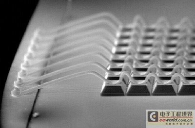
After the LEDs are bonded, wirebonds are used to complete the interconnection. High-density, high-frequency LED matrix formats require that the LEDs be interconnected using metal wires. Although there are a variety of wire bonding methods, such as ball bonding and wedge bonding, test data shows that chain bonding interconnection using a ball bonder gives the best results. For standard ball/pin bonding, a ball is formed first, and then the wire is pulled to the pin to bond to form the LED interconnection. Chain bonding is a variation of ball/pin bonding, where the pin is not a terminal, and a coil-pin combination is formed on it to complete the chain wire bond set. Figure 3 shows a chain bond using a wire bonder, setting up a ball-wire arc-intermediate pin-wire arc-intermediate pin-wire arc. The last is a wire arc pin, and then a ball pin is formed on each terminal pin to ensure the connection. This is not a new technology, but it has been further developed through material selection and software tools. Chain bonding allows for higher yields because it forms a standard ball bond without the need to form an air-free sphere. In addition, due to the chain-shaped solder pin pattern, there is less light occlusion, and the tensile test results prove that it has better pull-out strength.

Figure 3 Chain welding with safety connection
in conclusion
Assembling LEDs in a matrix can achieve higher density and higher brightness LEDs. This structure poses a challenge to packaging due to the high concentration of heat and the requirement for high-frequency wire bonding connections. Bonding wires must be placed accurately in areas where LEDs are densely packed, and the connection has a stable wire arc shape. Due to large thermal disturbances, the connection strength should also be strong enough to withstand mechanical shock and stress. There are three critical steps in the packaging process. The first step is to pick and place the chips with high precision to achieve matrix LED applications within the geometric tolerance of the LED . Second, it is necessary to apply pulse heating controlled batch eutectic reflow chip bonding processes for assembly production, LED protection, and good thermal conductivity, while providing high quality and low-risk performance. Third, chain connections provide excellent array electrical and mechanical connections for all LEDs. These packaging processes can achieve high brightness effects while also achieving heat dissipation and maximum light extraction efficiency.
Previous article:Implementing Precise Dimming LED Driver Design
Next article:Design of PFC switching power supply based on LED street lamp
Recommended ReadingLatest update time:2024-11-16 14:47


- Popular Resources
- Popular amplifiers
- MathWorks and NXP Collaborate to Launch Model-Based Design Toolbox for Battery Management Systems
- STMicroelectronics' advanced galvanically isolated gate driver STGAP3S provides flexible protection for IGBTs and SiC MOSFETs
- New diaphragm-free solid-state lithium battery technology is launched: the distance between the positive and negative electrodes is less than 0.000001 meters
- [“Source” Observe the Autumn Series] Application and testing of the next generation of semiconductor gallium oxide device photodetectors
- 采用自主设计封装,绝缘电阻显著提高!ROHM开发出更高电压xEV系统的SiC肖特基势垒二极管
- Will GaN replace SiC? PI's disruptive 1700V InnoMux2 is here to demonstrate
- From Isolation to the Third and a Half Generation: Understanding Naxinwei's Gate Driver IC in One Article
- The appeal of 48 V technology: importance, benefits and key factors in system-level applications
- Important breakthrough in recycling of used lithium-ion batteries
- Innolux's intelligent steer-by-wire solution makes cars smarter and safer
- 8051 MCU - Parity Check
- How to efficiently balance the sensitivity of tactile sensing interfaces
- What should I do if the servo motor shakes? What causes the servo motor to shake quickly?
- 【Brushless Motor】Analysis of three-phase BLDC motor and sharing of two popular development boards
- Midea Industrial Technology's subsidiaries Clou Electronics and Hekang New Energy jointly appeared at the Munich Battery Energy Storage Exhibition and Solar Energy Exhibition
- Guoxin Sichen | Application of ferroelectric memory PB85RS2MC in power battery management, with a capacity of 2M
- Analysis of common faults of frequency converter
- In a head-on competition with Qualcomm, what kind of cockpit products has Intel come up with?
- Dalian Rongke's all-vanadium liquid flow battery energy storage equipment industrialization project has entered the sprint stage before production
- Allegro MicroSystems Introduces Advanced Magnetic and Inductive Position Sensing Solutions at Electronica 2024
- Car key in the left hand, liveness detection radar in the right hand, UWB is imperative for cars!
- After a decade of rapid development, domestic CIS has entered the market
- Aegis Dagger Battery + Thor EM-i Super Hybrid, Geely New Energy has thrown out two "king bombs"
- A brief discussion on functional safety - fault, error, and failure
- In the smart car 2.0 cycle, these core industry chains are facing major opportunities!
- The United States and Japan are developing new batteries. CATL faces challenges? How should China's new energy battery industry respond?
- Murata launches high-precision 6-axis inertial sensor for automobiles
- Ford patents pre-charge alarm to help save costs and respond to emergencies
- New real-time microcontroller system from Texas Instruments enables smarter processing in automotive and industrial applications
- How to choose between mobile phone and tablet
- During electrical inspection, Warning Unconnected Power Object On Net GND appears
- Transfer - Dig deep into the magic of the smallest resistance and most versatile 0 ohm resistor to save your design
- MYC-CZU3EG core board information
- Analyzing the temperature sensor sampling circuit
- 【DFRobot motor driver】+Received DFRobot Arduino driver board
- EEWORLD University----How High-Voltage Isolation Technology Works
- New communication capabilities for TI's C2000 microcontrollers!
- At 10 am today, Keysight Technologies will broadcast a live broadcast on [Applications and Techniques of Oscilloscopes in the Electronics Industry]
- EEWORLD University ---- Live playback: Start your next-generation 4K display application design with TI DLP? technology

 Siemens PLC Project Tutorial
 LED Cube Code
 ESP32-S3 source code


 京公网安备 11010802033920号