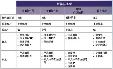
Touch screen is a mature technology, the most basic and most commonly used is the 4/5-wire resistive touch screen. Many standard screens support multiple sizes, and multiple decoding analog solutions can be selected. Resistive touch screens support multiple input methods, such as fingers, stylus, gloves and nails, etc. Capacitive touch screen is a new solution, also with 4/5-wire options, fewer standard screens, and fewer complex analog decoder solutions. Capacitive touch screens are more suitable for finger input, but not for nail, stylus and glove input. The main advantage of capacitive screens is surface durability. Mature resistive and capacitive touch screens are limited to single-point touch. Products such as iTouch use multi-touch technology, which increases the human-machine interface and adds more than two simultaneous inputs or touch points. Examples of static input touch include the Shift key and Control, Alt, Delete function keys on the keyboard or game controller, which have multiple independent controls; examples of dynamic input include gestures, commands, rotation movements or shrinking, expanding, etc. After using multi-touch technology, traditional touch technology seems too simple.
Currently, applications that can use multi-touch technology include medical imaging (needed for ultrasound, X-ray and MRI for image processing), information inquiry terminals (photo printing, retail information inquiry terminals, maps/navigation, etc.), music/video players (iTouch), home appliances, etc. This article will introduce a simple digital low-cost alternative to implement a multi-touch system using a digital resistive touch screen and MAX II CPLD.
Multi-touch decoding
Any multi-touch solution starts with a touch screen. The example in this article uses the digital SmartTouch from NKKSwitch, model FTAS225-5.7AN. There are other digital resistive screens of different sizes from other suppliers. The processing interface is I2C, but other interfaces can also be used.
The FTAS225-5.7AN uses a 5.7” laminated screen with 15 rows x 15 columns and a touch resolution of 5mm x 7mm. The screen stack is actually a 15 x 15 switch matrix. The digital resistive screen stack uses horizontal and vertical Iridium Tin Oxide (ITO) traces. The traces are separated and short the two layers when touched.
For this demonstration, the design is simplified to an 8 x 8 digital resistive touch screen. This example uses the processor I²C interface, but any serial or parallel interface can be provided for any processor. This design only requires the MAX II to connect the digital resistive touch screen to the processor, using the MAX II internal pull-up resistors and internal oscillator reduce external components.
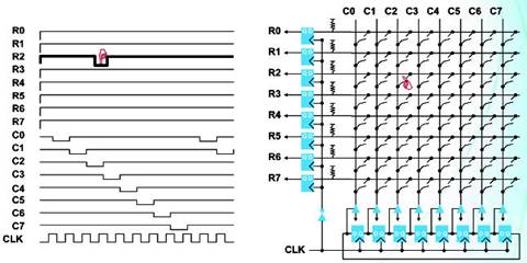
In Figure 1, the vertical register samples each row at each column, and the horizontal register forms a shift register, and the array is driven low each time. The waveform in the figure shows how the screen is decoded when there is no touch. When no point on the screen is touched, the row detection signal remains high. When the second row and second column on the screen is touched, it causes the second row to be pulled low during C2 sampling. Each time the display is scanned, the I2C module sends 8 bytes of data to the processor.
 |
|
Table 1 Advantages and disadvantages of touch screen |
 |
|
Figure 1: Single-touch decoding working mode |
How does multi-touch decoding work? The waveform in Figure 2 shows three touch points. The finger symbols in the figure show how each touch point is mapped to the row and column sample signals. Three touch points result in three low pulses during scanning. Under certain 3-finger touch conditions, the simple decoder will incorrectly report the presence of aliased signals, which is an incorrect touch point decoding. The three touch points must form a triangle with two points sharing a row and two points sharing a column. The red circled lines in the figure show the aliased signal decoded pulses.
|
Figure 2 Multi-touch decoding working mode |
The improved decoder circuit can reduce or even eliminate aliasing signals. First, we need to increase the clock rate, usually by 10-100 times. In Figure 3, the I2C clock is increased from 100kHz to 4MHz. Synchronous shift and sample enable signals (green) are added. SFT is the shift enable signal, and SEN is the sample enable signal. A timing control module is added to support SFT to SEN delay adjustment (red) and support shift enable signal sampling enable delay adjustment. The timing control module can reduce the shift enable sampling, and the enable delay can increase the shift enable. The sample enable delay controls the delay of each column and each row independently.
|
Figure 3 The improved circuit reduces aliasing signals (1) |
How does the circuit remove the aliased signal? In the actual system, the timing is not adjusted, and the clock is faster. RA to RE details the touch screen path that generates aliased signals, including the ITO trace impedance and I to RE. I to RE details the touch screen path that generates aliased signals. Due to the use of resistors, the delay from finger touch point 1 to the aliased signal pulse is relatively large, so controlling the sampling enable timing will ignore it. As shown by the arrow in the lower left, by improving the sampling enable signal, the aliased signal can be eliminated. Figure 5 shows the delay and timing changes in detail. The clock frequency is still slower than the actual example to facilitate the understanding of the figure. The sampling timing of columns 0 and 5 is different to eliminate aliased signals. Although the C5 SEN signal lags behind the C0 SEN signal, it is still much shorter than the original design. The designer's goal is to make the sampling timing of each column and each row long enough to correctly sample the real touch, but short enough to ignore the aliased signal according to the characteristics of the touch screen and PCB. Using the programmable capabilities of MAX II devices, designs can be quickly reconfigured or dynamically controlled using JTAG, making it easy to adjust circuits.
|
Figure 4 The improved circuit reduces aliasing signals (2) |
|
Figure 5 The improved circuit reduces aliasing signals (3) |
The reference design board is very simple (Figure 6). Simply connect the MAX II device directly to the 30 pins of the touch screen and the 15×15 LED array. There is also a download connection line J1 and an expansion header J3 for SPI or I2C connection. Compared with the I2C interface, the LED array is easier to use for interactive demonstrations.
|
Figure 6 Demonstration circuit board schematic |
Figure 7 is a block diagram of the MAX II circuit. It includes a shift register with shift control signals from the timing control block. The timing control block also controls the sampling register. To effectively demonstrate the effects of timing changes, the JTAG Source Probing Feature Mega Wizard and the Source Probing Editor supported by the Quartus II and MAX II families will be used.
|
Figure 7 MAX II circuit diagram |
As shown in Figure 8, the timing control module has 4 states, which are shown in the lower left corner. "Reset" drives all pins high, with a setup time of 16 clock cycles. "Shift" moves the column scan to the left. "Wait" is a programmable delay from shift to sampling. The JTAG8 module controls the delay, which is an 8-bit value downloaded from the JTAG cable, and the control comes from the Quartus Source Probe Editor window. It also samples internal nodes so that they can be read in real time in Quartus. After the "Wait" cycle, the Sample state collects the column data.
|
Figure 8 Timing control module |
MAX II is a programmable logic device that can be easily customized using the free Quartus II design tool to meet the user's application needs. At the same time, MAX II CPLD has the following features, which are very suitable for digital resistive touch screen decoding: a large number of I/O pins, including 160 I/Os in the ultra-low power MAX IIZ series and 272 I/Os in the MAX II series. Few processors provide enough I/Os to decode digital resistive touch screens; all MAX II devices have internal oscillators and programmable internal I/O pull-up resistors; MAX II devices support in-system programming, so that printed circuit boards can be designed first and then the timing can be adjusted; MAX II has very low power consumption, and MAX IIZ is suitable for many battery-powered portable applications; finally, programmable MAX II can flexibly support processors that require standard or dedicated interfaces.


 Synaptics_RMI3_Specification
 Panasonic PLC routine_Paper clip type Touch Screen sample machine
 Youlong\'s ARM9 FS2410 development board original code


 京公网安备 11010802033920号